PROGRAMMING
When you're dealing with computer logic, things can get very complicated very fast. This is especially true when it comes to address decoding. You can easily find yourself tangled in a messy web of AND, OR, NAND and NOR gates.
And there's a problem you're likely to run into when stringing together a bunch of logic gates — propagation delay. It takes a measurable amount of time for a chip to convert input into output. If there's only one chip involved then you live with it. But if your signals have to traverse a sequence of three or four chips before you get the logical output you want, then that can cause problems. A general rule of thumb is to keep decoding logic to being two layers deep — three at most, if you're running a low-speed system.
And just getting all those logic chips arranged on a PCB can be a pain.
A chip of your own
This is where programmable logic comes to the rescue. We've had various kinds of programmable logic chips for decades. Some of these devices — such as GALs — are finally fading away. But Complex Programmable Logic Devices (CPLDs) and their big brothers, Field Programmable Gate Arrays (FPGAs) remain highly popular.
With an FPGA, you can effectively replace an entire computer's worth of chips with just one IC. But here we'll be looking at a somewhat simpler device — the CPLD.
To be precise, I'll describe my experience in replacing six logic chips with one CPLD through the cunning use of an Atmel ATF1502AS and the CUPL hardware description language introduced by Logical Devices. So when I say that this is a 'beginner's experience', I mean that I'm the beginner and this is the experience I gained in my first encounter with CPLDs.
But first, let's get something out of the way. When you 'code' for a programmable logic device — whether it's in CUPL, Verilog, VHDL or some other things I'm no expert in — you're not writing a 'program'. You're creating a description of a piece of hardware — the logic operations it performs and how the various gates, inverters and whatnot link together. And so purists can get upset when you use terms like 'program'. With FPGAs, for example, you don't compile your code, you 'synthesise' it. (Interestingly, CUPL does use the term 'compile').
But I'm new to all this, so I'm going to stick with terms like 'code', 'programming' and 'compile' because I'm comfortable with those.
How do you do it?
The first challenge you're likely to meet is just getting good quality information on how you go about programming CPLDs and the toolchain you need to do it. I believe it is possible to employ the tools intended for FPGAs — software such as Quartus and languages like Verilog — to program CPLDs. But that steepens the learning curve considerably.
Here's the bad news. I haven't yet found any sensible way of doing this under any operating system other than Windows. Ugh!
WinCUPL. Just say no.
You're going to find yourself steered towards WinCUPL, a GUI-based program from Atmel (now Microchip) that, seemingly, hasn't had so much as a lick of paint since the Windows XP days. It's crashy and buggy and, as far as I'm concerned, not worth using.
You'll still need to install it, though, to get the tools that come with it — it's just that, if you're smart, you'll end up using CUPL from the command line. Also, on the same download page you'll find ATMISP — a utility for burning the code to the chip. This does its job reasonably well, so go grab that.
Good tutorials are surprisingly hard to come by. I've included a bunch of references below that you may find useful.
Experimental setup
Next, we have to talk about how you talk to the CPLD, to program it. Some CPLDs come in DIP packages, which are easy to play with on a breadboard. Others are in PLCC or TQFP formats, which aren't so convient. Typically, you're going to program the chip via a JTAG interface and will most likely need a programmer device of some kind. The variations here are immense — too many to deal with here, so I'll just tell you what set-up I used.
I bought an Atmel ATF15XX-DK3 development board. This takes 44-pin TQFP versions of the two chips that most interest me — the ATF1502AS and ATF1504AS (two 1502 chips are included with the board). It has LEDs, 8-segment displays and push-buttons that you can use when developing code, or just to muck about. But you can also ignore them if you wish. The board can be set for various voltages, so, for example, you can use the 5V and 3.3V versions of the chips. And there are adapters available for using chips in other packages. It's a great way to learn about CPLDs.
I also got the Microchip ATDH1150USB programmer which, as its name suggests, connects to a PC via USB and offers JTAG-A, JTAG-X and TWI outputs.
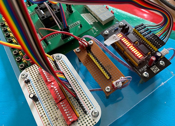
To augment these, I made up a few breakout boards. Using stripboard, I created a power distribution board which takes power from the DK3 and provides it via rows of DuPoint headers. As we as providing power to my other breakout boards, it's a way of tying signals high or low.
Using a prototyping board, I set up a row of 24 DIP switches to emulate an address bus, a data bus or other signals.
And I also have a board with 16 LEDs, driven via a buffer, to show outputs from the CPLD.
Getting to know CUPL
This is not going to be a CUPL tutorial. It's just my experience. However, the truth is I came into this feeling quite daunted by the language and its concepts, but quickly got to the point of thinking, "oh, is that all there is?".
Well, no. I managed to write three working pieces of code in a day, but I realise I've only scratched the surface of what it can do.
But before we get ahead of ourselves, let's look at what I wanted to achieve.
The goals
I designed and built my own 8-bit, 6502-based computer — the Zolatron 64. I'll be getting into that through a whole series of articles coming soon.
My initial address decoding scheme for the Zolatron 64 had eight addresses for I/O. But these are 1KB apart, which seems wasteful. You can get over-obsessed with highly granular decoding, but I wanted something a little more sophisticated. I decided to keep the current 1KB slots but also allocate another eight slots just 32-bytes apart. These actually sit in the top part of the uppermost 1KB slot.
If you're not familiar with address decoding, here's a highly simplified version of what it does.
A computer has an address bus. In the case of the Zolatron, this is 16 bits wide. You can think of it as 16 wires running in parallel that attach to the 16 address pins of the processor chip. These wires also run to a whole bunch of other chips, such as ROM and RAM. But what we're concerned with here are I/O devices such as a serial communications chip. The 16 wires constitute a 16-bit binary number. Depending on which bits are high and which are low, you can get the processor to set an address from 0 to 65,535 (or 0x0000 to 0xFFFF if you prefer hexadecimal).
In an address-based architecture, you arrange 'decoding logic' (often referred to as 'glue logic') that sees this address and interpets it. A given address will have a particular pattern of bits that are high and low. Decoding logic converts this pattern and outputs signals accordingly.
Let's taken the classic example of the 74xx138 decoding chip, which is what I already use for some of the decoding on the Zolatron. You connect carefully selected lines from the address bus to its inputs (not all the lines — just ones you're particularly interested in). The 74xx138 has eight outputs and, by default, these are all set high. But if the inputs fall into a particular pattern, one of the outputs (and only one) will go low. So you can decide which one goes low by selecting a specific address.
The kinds of chips you use for I/O typically have an 'enable' pin. You set this to a specified state (usually low) to activate the chip. If it's not activated, then the chip ignores everything that's going on and keeps itself to itself. So, using a 74xx138, you can select (address) one of up to eight other chips simply by setting an address on the address bus.
More addresses
I use the 74xx138 to select the eight main I/O addresses on the Zolatron. But I also wanted to be able to select a Flash memory chip — an SST39SF0101A — that sits at address $8000. That address gets selected when A15 is high and both A14 and A13 are low. As is common, its chip enable pin is active low (/CE).
I also wanted to create eight more addressable I/O devices, each of which would occupy a 32-byte slot in the memory map.
In the Zolatron 64's memory map, that address is the start of an 8KB block. But the Flash chip is capable of holding 128KB. For this reason, it has address pins A0-A16.
Now, we could use a few logic gates to ensure a low signal when A13-A15 are in the appropriate states and just use the lowest 8KB of the flash chip. But that's very wasteful.
Instead, what I want to be able to do is treat the Flash memory as 16 'banks', each 8KB in size. Once a bank is selected, I want it to remain the active bank until such time as I select a different one. Which is why the word 'latch' is marching steadily towards this article.
The idea is that selecting the bank is a simple matter of writing a value (0–15, or 0x00–0x0F) to a memory address — ie, one of the new 32-byte I/O addresses. I chose the address $BFE0. That address is selected when A14 is low and A15 plus A13-A8 are high. Note how that means seven address pins need to be high at the same time. Checking for that state using discrete logic ICs could get messy. Plus you have to add the low A14 into the mix and qualify everything with a high clock state.
What I need is for four inputs pins (giving values in the range 0–15) to control the pattern of four output pins, which are connected to address pins A13-A16 on the Flash chip. That's how you select which bank to use. And those output pins need to be latched.
Now, you can do this sort of thing with all manner of latches, but then we still have the messy decoding issue. A CPLD makes it simple to do everything in one place.
Implementing the logic
The 'code' you write in CUPL describes what the hardware should do. The CUPL compiler then works out how to achieve that. Let's look at it piece by piece.
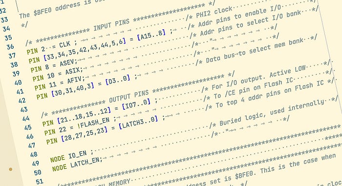
/* *************** INPUT PINS ******************** */
PIN 2  = CLK ;                       /* PHI2 clock                     */
PIN [33,34,35,42,43,44,5,6] = [A15..8] ;   /* Addr pins to enable I/O        */
PIN 8 = ASEV;                        /* Addr pins to select I/O bank   */
PIN 10 = ASIX;                      /*   "         */
PIN 11 = AFIV;                      /*   "         */
PIN [30,31,40,3] = [D3..0] ;            /* Data bus to select mem bank  */
Here we've assigned input pins. These assignments give the pins names we can use in our logic, such as CLK, A15, A14 etc.
The CLK is connected to the computer's PHI2 clock signal. The next lots of pins are connected to address bus signals. Note how we can declare a range [A18..8] to designate an indexed series of labels, much like an array. Three more address signals get pin assignments. Why not include these in the previous array? Because there are operations we want to carry out later where you're not allowed to mix ordinary names with indexed ones. Finally, we link four pins to the lowest four data bus signals.
/* *************** OUTPUT PINS ******************** */
PIN [21..18,15..12] = [IO7..0] ;            /* For I/O output. Active LOW     */
PIN 22 = !FLASH_EN ;                  /* To /CE pin on Flash IC         */
PIN [28,27,25,23] = [LATCH3..0] ;         /* To top 4 addr pins on Flash IC */
The output pins are fairly self-explanatory. We have the eight I/O pins, a /FLASH_EN pin which will be set low when we want the Flash chip to be active, and the four latched and decoded pins that go to the top four address pins of the Flash chip.
Note how FLASH_EN is defined with ! in front of it. This says that this signal is active low — or, put another way, when the conditions that make FLASH_EN true exist, that output signal will be low, but otherwise will be high.
There's one tip I have to offer here. If you assign pins manually like this, you might find the compiler complaining about your choices. Not all the I/O pins on a CPLD chip are equal in capabilities, and some are input-only. If you find this happening, remove the numbers from some of the assignments. For example, instead of:
PIN [21..18,15..12] = [IO7..0] ;You could put:
PIN = [IO7..0] ;What will happen is that the compiler will choose pins for you. But you're not stuck with its choices. You can see which pins it thinks are appropriate and use that as a guide, swapping them around to suit your circuit board layout.
You can see which pins the compiler has chosen in the .fit file created during compilation. This lists the pins and also draws a handy little diagram, like this:
                 A  A  A  V              G  A  A
                 1  1  1  C  D           N  1  1
                 0  1  2  C  1           D  3  4
               ____________________________________
              /  44 43 42 41 40 39 38 37 36 35 34  \
         TDI |  1                                33 | A15
         CLK |  2                                32 | TDO
          D0 |  3                                31 | D2
         GND |  4                                30 | D3
          A9 |  5                                29 | VCC
          A8 |  6            ATF1502             28 | LATCH3
         TMS |  7          44-Lead TQFP          27 | LATCH2
        ASEV |  8                                26 | TCK
         VCC |  9                                25 | LATCH1
        ASIX | 10                                24 | GND
        AFIV | 11                                23 | LATCH0
             |   12 13 14 15 16 17 18 19 20 21 22   |
              \____________________________________/
                 I  I  I  I  G  V  I  I  I  I  F
                 O  O  O  O  N  C  O  O  O  O  L
                 0  1  2  3  D  C  4  5  6  7  A
                                               S
                                               H
                                               _
                                               E
                                               N
The compiler creates lots of files, with .fit and .doc (a plain text file, whatever Windows tells you) being among the most informative.
The in-between bit
We've got inputs and we've got outputs. But the real magic happens in-between.
NODE IO_EN ;
NODE LATCH_EN;
I added a couple of nodes. You can think of nodes as internal 'pins'. You can't connect to them physically, but you can use them as intermediate points in the logic. A node could be a single item or an indexed array, just like pins.
/* *** FLASH MEMORY *** */
FLASH_EN = A15 & !A14 & !A13 ;               /* Chip enable    */

LATCH_EN = A15 & !A14 & [A13..8]:& & ASEV & ASIX & AFIV ;

LATCH3.d = D3 ;                     /* D-latch input           */
LATCH3.ck = CLK & LATCH_EN ;        /* Address-qualified clock */
LATCH2.d = D2 ;
LATCH2.ck = CLK & LATCH_EN ;
LATCH1.d = D1 ;
LATCH1.ck = CLK & LATCH_EN ;
LATCH0.d = D0 ;
LATCH0.ck = CLK & LATCH_EN ;
And now for some actual logic.
First, we set FLASH_EN to be true when A14 is low, and A15 and A13 are high (address 0x8000). Note that we're dealing in matters of True/False here, not pin voltages. Because we defined FLASH_EN as active low earlier (!FLASH_EN), when this statement is true, FLASH_EN will be low.
The LATCH_EN statement is a little trickier. We're about to set up four D-type latches to set and hold our signals to the top four address line of the Flash memory. The way a D-latch works is that, whenever the CLK signal is high, the output of the latch (usually given the designation D), is set to match the input. When the clock goes low, the latch holds on to the last value it received.
But we don't want the outputs of the latches simply to follow the inputs every time the clock is high. We want this to happen only when we're writing to the address 0xBFE0. And so we 'qualify' the clock signal with some address decoding. If A14 is low, and A15-A5 are all high, this selects the address 0xBFE0. By ANDing this decoding with the CLK signal, we ensure the latches' clock signals are high only when that address is selected and the clock is high. And we do this decoding by specifying how the LATCH_EN node we defined earlier behaves according to various inputs.
We describe the latches with so-called 'extensions'. The .d extension tells the compiler which input signal the output of the latch should follow. The .ck extension specifies which is the clock signal.
Also note one little bit of cleverness in the LATCH_EN definition:
[A13..8]:&This is shorthand for saying AND all the pins from A13 down to A8. It just makes the line a lot shorter than:
A13 & A12 & A11 & A10 & A9 & A8Not so fast
It turns out, though, there's a problem with the above code, which was pointed out to me when I first shared it online. I've left the error in so that we can learn from it.
The issue is to do with how I've defined the latches.
LATCH3.d = D3 ;                 /* D-latch input           */
LATCH3.ck = CLK & LATCH_EN ;    /* Address-qualified clock */
The issue here is one of timing. With a D-type latch, which is what we have here, the value of the output is set when the clock goes from low to high — ie, a rising edge. But the 6502's data bus is not guaranteed to be stable at that point. We really need to trigger the latch value on the falling edge.
There are two ways of doing this. One is to use an L-type latch. In this case, whenever the clock is high, the output matches the input — the latch is said to be transparent. The value gets latched when the clock goes low. This means that if the input value changes while the clock is high (which it might if the data bus is still settling down), the latch value will also change before the latchng mechanism comes into effect. It gives the data bus a bit more time to get itself sorted out.
To do this, we change the latch definition this way:
LATCH3.l = D3 ;
LATCH3.en = CLK & LATCH_EN ;
Now we have an L-type latch that is enabled by the clock and LATCH_EN signals.
The other method is to use a D-type latch but invert the clock signal so that the latch triggers on a falling edge rather than a rising edge. That's actually what I doing in a later version of this code, but we'll save that for another day.
And that's it for the Flash memory. In my 6502 assembly code, I can now use something like this:
FLASH_SEL = $BFE0

; ...

lda #10 ; To select Flash bank 10
sta FLASH_SEL
Selecting I/O
The last section of the CUPL code involves our I/O select lines. Remember, we want just one line to be low at a time.
/* *** EXTENDED I/O *** */
IO_EN = A15 & !A14 & [A13..8]:& & CLK;       /* PHI2-qualified addr decode */
FIELD DEV_ADDR = [IO_EN, ASEV, ASIX, AFIV] ; /* Address state              */
FIELD DEV_SELECT = [IO7..0] ;                /* I/O output state           */

TABLE DEV_ADDR => DEV_SELECT {     /* Match addr state to I/O output state */
'b'0XXX => 'b'11111111 ;           /* If IO_EN false, no output selected   */
'b'1000 => 'b'11111110 ;           /* Selected output is LOW               */
'b'1001 => 'b'11111101 ;           /*    "                                 */
'b'1010 => 'b'11111011 ;           /*    "                                 */
'b'1011 => 'b'11110111 ;           /*    "                                 */
'b'1100 => 'b'11101111 ;           /*    "                                 */
'b'1101 => 'b'11011111 ;           /*    "                                 */
'b'1110 => 'b'10111111 ;           /*    "                                 */
'b'1111 => 'b'01111111 ;           /*    "                                 */
First, we define that the IO_EN node should be true (high, in this case) whenever A14 is low and A15 plus A13-A8 are high and the clock is high.
We then include this IO_EN signal with three address signals — ASEV, ASIX and AFIV — in what's known as a FIELD, which I've called DEV_ADDR. In this case, you can think of a field as either the rows or columns of a table, as we'll see in a minute. This field is why I labelled these address signals 'ASEV' etc. If I tried to use A7, the compiler would complain that I was trying to mix indexed signals (A7, A6, A5) with non-indexed ones (IO_EN). Any designation ending with a number is assumed to be indexed.
The DEV_ADDR field will act as inputs.
We create another field, DEV_SELECT, to provide the outputs. These consist of the eight outputs pins defined at the start. Here we can use indexed values [IO7..0] because they are all indexed items.
Finally, we build a truth table where input states in DEV_ADDR are matched to output states in DEV_SELECT. The left-hand column consists of all the combinations of signals in DEV_ADDR — or, at least, the combinations we care about. You can see that the first says:
'b'0XXX => 'b'11111111 ;The Xs stand for 'don't care'. In this case, if the IO_EN signal is false, then it doesn't matter what state the three address signals are in — we're just going to set all the output signals high. But when the IO_EN signal is true, the output signals will be set according to the state of the address signals — eg:
'b'1010 => 'b'11111011 ;When IO_EN is true, ASEV is low, ASIX is high and AFIV is low, set IO2 to low and all the other IO pins to high. The 'b' stipulates that the number given is in binary notation.
Working prototype
Getting the code on to the chip was a bit of a struggle at first. I fought with WinCUPL far longer than I should, until a kind soul on 6502.org pointed me to a script that allows you to compile from the Windows command line.
I've since seriously amended this script. It works for the ATF1502AS and ATF1504AS CPLDs. It assumes that the name you've put in the headers of your code (FLASHDECODE in the example below) is the same as the source filename (FLASHDECODE.PLD), the name of the script (FLASHDECODE.cmd) and also the same as the name of the directory the source is in. The script also needs to live in and be run from that directory. I'm sure I could be a lot smarter about this, but I don't much care for Windows and am no scripting wizard on this platform.
The script also needs a hard-coded path to wherever you've installed cupl.exe.
@ECHO OFF
REM Make sure this script name is identical to both the folder name
REM and the filename of the .pld and .tt2 files.
REM Also, edit the CPLD variable to suit the chip

set CPLD=1502

if %CPLD% equ 1502 (
    set CHIPDES=f1502tqfp44
    set DEV=P1502T44
) else if %CPLD% equ 1504 (
    set CHIPDES=f1504tqfp44
    set DEV=P1504T44
) else (
    exit 1
)
ECHO Compiling for %CPLD%
ECHO Running cupl.exe...
C:\Wincupl\Shared\cupl.exe -j -a -l -e -x -f -b -m4 %CHIPDES% %~n0
if %ErrorLevel% equ 0 (
    ECHO Running find...
    if %CPLD% equ 1502 (
        find1502 -i %~dp0\%~n0.tt2 -CUPL -dev %DEV% -str JTAG ON -str logic_doubling off
    ) else if %CPLD% equ 1504 (
        find1504 -i %~dp0\%~n0.tt2 -CUPL -dev %DEV% -str JTAG ON -str logic_doubling off
    )
)
This script spits out all the files you need — in particular, the .jed JEDEC file which is what you feed to ATMISP to burn the code to the CPLD.
This article has rolled on much longer than I anticipated. I wanted to set down the lessons I learned while I still remember them, so that I can come back here in a month's time when I've forgotten how to do this. However, I feel like I've still glossed over a bunch of stuff, so if you have questions, please ask. I'm no expert, but I am a veteran of the lower parts of the learning curve.
Full code
Here's the code in full:
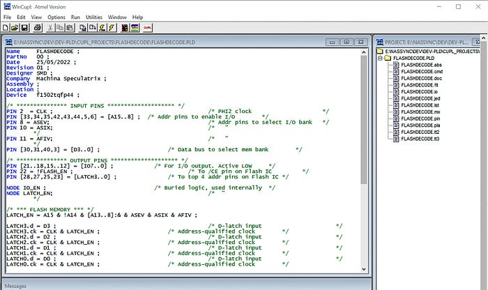
Name     FLASHDECODE ;
PartNo   00 ;
Date     25/05/2022 ;
Revision 01 ;
Designer SMD ;
Company  Machina Speculatrix ;
Assembly ;
Location ;
Device   f1502tqfp44 ;

/*

Provides the necessary decoding for a Flash memory device on the Zolatron 64.
The Flash memory lives at address $8000.
It also provides a latched bank selector at address $BFE0. Writing a value 0-7
to this address sets the values of three address pins (5-7) on the Flash
device, effectively selecting one of eight 8K memory 'banks'.

This program also decodes address for the eight extended I/O lines on the
Zolatron 64 data bus. This decoding enables a clock-qualified chip enable
signal (active low) at 32-bit intervals. The addresses are:
  $BF00, $BF20, $BF40, $BF60, $BF80, $BFA0, $BFC0, $BFE0.

*/

/* *************** INPUT PINS ******************** */
PIN 2  = CLK ;                             /* PHI2 clock                     */
PIN [33,34,35,42,43,44,5,6] = [A15..8] ;   /* Addr pins to enable I/O        */
PIN 8 = ASEV;                              /* Addr pins to select I/O bank   */
PIN 10 = ASIX;                             /*   "                            */
PIN 11 = AFIV;                             /*   "                            */
PIN [30,31,40,3] = [D3..0] ;               /* Data bus to select mem bank    */

/* *************** OUTPUT PINS ******************** */
PIN [21..18,15..12] = [IO7..0] ;            /* For I/O output. Active LOW     */
PIN 22 = !FLASH_EN ;                  /* To /CE pin on Flash IC         */
PIN [28,27,25,23] = [LATCH3..0] ;         /* To top 4 addr pins on Flash IC */

NODE IO_EN ;                                /* Buried logic, used internally  */
NODE LATCH_EN;                      /*  "         */

/******************************************************************************
*****   FLASH MEMORY                                                      *****
*******************************************************************************/
/* LATCH_EN is selected when the address set is $BFE0. This is the case when
we're writing a value to select the memory bank. */

LATCH_EN = A15 & !A14 & [A13..8]:& & ASEV & ASIX & AFIV ;

/* The individual D-latches for the inputs from the data bus have their clocks
enabled (allowing the flip-flop to be set to the appropriate value) only when
the main clock is high and LATCH_EN is active. */
LATCH3.l = D3 ;                                      /* D-latch input       */
LATCH3.le = CLK & LATCH_EN ;              /* Address-qualified clock        */
LATCH2.l = D2 ;
LATCH2.le = CLK & LATCH_EN ;
LATCH1.l = D1 ;
LATCH1.le = CLK & LATCH_EN ;
LATCH0.l = D0 ;
LATCH0.le = CLK & LATCH_EN ;

/* Chip enable is active when the address $8000 is set. */
FLASH_EN = A15 & !A14 & !A13 ;                         /* Chip enable       */

/******************************************************************************
*****   EXTENDED I/O                                                      *****
*******************************************************************************/
IO_EN = A15 & !A14 & [A13..8]:& & CLK;        /* PHI2-qualified addr decode */
FIELD DEV_ADDR = [IO_EN, ASEV, ASIX, AFIV] ;  /* Address state              */
FIELD DEV_SELECT = [IO7..0] ;                 /* I/O output state           */

TABLE DEV_ADDR => DEV_SELECT {  /* Match address state to I/O output state  */
'b'0XXX => 'b'11111111 ;        /* If IO_EN alse, then no output selected   */
'b'1000 => 'b'11111110 ;        /* Selected output is LOW                   */
'b'1001 => 'b'11111101 ;        /*    "            */
'b'1010 => 'b'11111011 ;        /*    "            */
'b'1011 => 'b'11110111 ;        /*    "            */
'b'1100 => 'b'11101111 ;        /*    "            */
'b'1101 => 'b'11011111 ;        /*    "            */
'b'1110 => 'b'10111111 ;        /*    "            */
'b'1111 => 'b'01111111 ;        /*    "            */
}
Like I said, this was my first encounter with CPLDs and CUPL. And it worked. But I'm not using this code. I've since dropped the idea of using Flash memory in the Zolatron. But I did develop this code further for the address decoding part, and I'll get into that more deeply when I start writing about the Zolatron.
I hope, at least, the details of my first tussle with CUPL will help you with yours.
Resources
- WinCUPL, Microchip Technologies, download page.
- CUPL Programmer's Reference Guide. (PDF). Based on Logical Devices' original guide, this is a slightly amended and improved version from the University of Southern California. Still has some typos, though (2012).
- Atmel WinCUPL User's Manual. (PDF) If you absolutely have to use WinCUPL.
- Atmel ATF15xx Family Series. (PDF) Overview of Atmel's CPLD devices.
- Atmel ATF15xx Family: ISP Devices: User Guide. (PDF). A very helpful a readable manual for using these devices.
- ATF15xx-DK3 CPLD Development/Programmer Kit: User Guide. (PDF). The essential manual for using the DK3 development board.
Steve Mansfield-Devine is a freelance writer and photographer. You can find photography portfolio at Zolachrome, buy his books and e-books, or follow him on Bluesky or Mastodon.
You can also buy Steve a coffee. He'd like that.
My Friend retro games NES SEGA