
RETROCOMPUTING
Well, that wasn't easy. Have you ever had one of those projects where you thought you'd overcome all the major hurdles only to find yourself going backwards?
This one was like that, with the added complication that it was a combination of new hardware and new software — two lots of software, in fact, in C++ and Python. Every time there was an issue it was hard to know where the fault lay. So let me take you through the process, and how I tried to pin down the problems.
In the end it was both a triumph and … aah no, we'll get to that soon enough.
Office bound
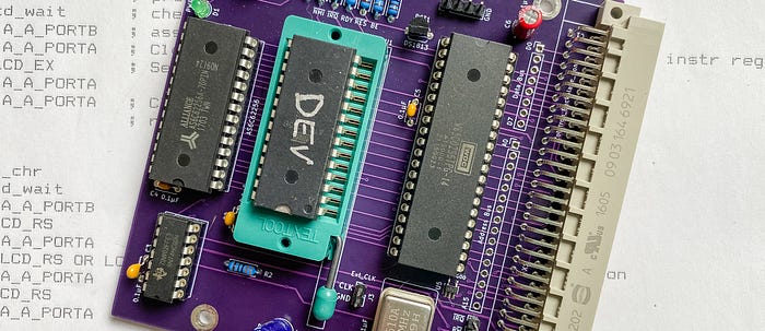
It started out as a straightforward concept — or so I thought. The Zolatron 65C02-based homebrew computer currently uses an EEPROM as its read-only memory (ROM). And that's fine. It works well enough.
But it's inconvenient. Every time I want to upgrade the ROM code (the machine's operating system), I have to shut off the machine, pull the EEPROM chip from its socket, place it in a programmer device, flash the new firmware, remove the chip from the programmer, place it back in its socket and turn the power back on.
And as long as that sentence was, actually doing those things takes a lot longer, especially when the flashing of the software doesn't work first time.
Worse, I have to be present. The Zolatron, dev machine and programmer all have to be there right in front of me, which means I'm tied to the office.
The concept
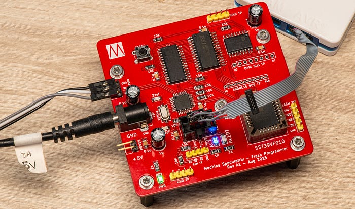
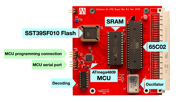
By replacing the EEPROM with flash memory, the chip can remain in place on the Zolatron's CPU board. I just needed some way of reprogramming it in situ, and the perfect solution for that is to have a microcontroller (MCU) on the board, too.
The MCU — an ATmega4809 — runs a program that listens for commands coming over a serial connection from my dev machine (a 2012 MacBook Pro running MX Linux, for the curious). When it receives a 'BURN' command, it downloads the new ROM code from the dev machine and writes it to the flash (an SST39SF010A chip). The MCU code has a couple more tricks, such as the ability to read sections of the flash ROM's memory, but the programming is the important bit.
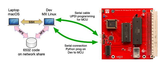
The dev laptop (which remains permanently in the office and which I generally access via SSH) does its part of the task using a Python script, itself callable from other scripts.
The 6502 ROM code is on a network share, so I can tweak it while sitting on the living room sofa or in the garden and reflash the Zolatron over an SSH session. Sweet.
But getting to this point wasn't easy.
First steps with flash
I documented my experiments with using flash memory in this way in a series of articles:
- Using flash memory as a homebrew computer ROM, which covered the basic concept and a breadboard-based prototype.
- A development board for flash-based ROM, where I covered designing a PCB based around an ATmega328PB microcontroller, SRAM and a flash chip.
- Software for the flash ROM development board, which I think is probably self-explanatory.
- Alternatives to ROM for a homebrew computer, where I applied the lessons learned to thoughts about how I could replace the EEPROM in the Zolatron.
I came to realise that the 'straight-to-flash' approach was most likely to succeed and I honed in on the ATmega4809 as the microcontroller for the job, mainly because it has lots of GPIOs.
Controlling the CPU
While the proof of concept experiments had worked well, there were always going to be some complications with moving the idea into the environment of the Zolatron.
It was important that the machine shouldn't have to be shut off before flashing the new code. That meant the computer would be running. And that creates issues.
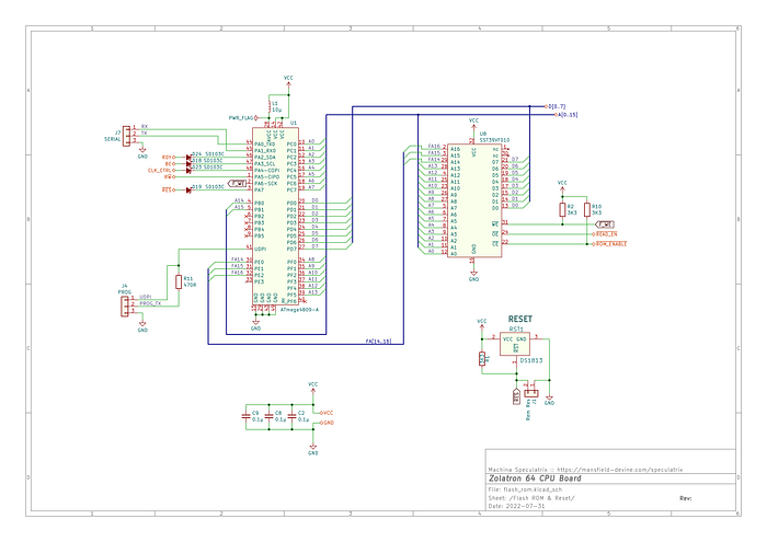
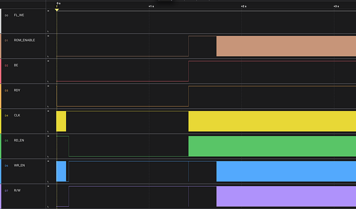
With the CPU still operating, it would be throwing out signals on the address and data buses. But to program the flash chip, the MCU would need sole control over those lines. The same goes for the CPU's read/write signal (RWB, aka R/W) which is crucial in the decoding logic to tell the ROM (ie, the flash chip) when it should be reading or writing.
Similarly, there are other signals employed by the decoding logic that we can control from the MCU. When address lines A14 and A15 are high, that activates the ROM (via the decoding chip). And the /READ_EN (read enable) and /WRITE_EN signals depend not just on the state of the RWB signal but also the clock, PHI2. They are active only when the clock is high, which is why PHI2 is an input to this decoding logic.
Luckily, the 65C02 CPU has some handy inputs that stop it from working — which in our case is a good thing.
Taking the BE (bus enable) input low makes the CPU let go of the address and data buses and the RWB pin, making them high impedance so that the CPU has no influence on those lines.
Pulling the RDY pin low halts the CPU (without it catching fire) and freezes it in whatever state it was in. Both the BE and RDY lines have been largely ignored in the Zolatron so far, other than being pulled high with 3.3KΩ resistors. Now it's their time to shine.
Both signals are behind Schottky diodes so that the MCU can only pull them low. The same goes for a GPIO connected to the system-wide /RESET line. This enables the MCU to reset the Zolatron after a firmware update.
Stopping the clock
Above, I mentioned how the clock, PHI2, is a key part of the decoding logic. But it's not a CPU output—it comes from the clock circuit. Somehow, we need to stop the clock.
This is done by introducing an extra bit of logic, in the form of a single, dual-input NAND gate. The signal coming out of the clock circuit is one input. A signal controlled by the MCU (which I'm called CLK_CTRL) is the other input. There is a Schottky diode in the CLK_CTRL line so that the MCU pin can only pull this line low, not drive it high (ie, it's effectively open drain). I also have a pull-up resistor on this line (22KΩ, which might be a little weak but seems to be working okay).
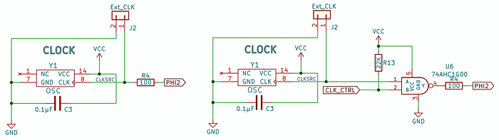
In normal use, the CLK_CTRL input will be high and the NAND gate will operate as a simple inverter—when the clock input is high, the output (PHI2) is low and vice versa. Inverting the clock is fine because this is the common clock source for everything.
If CLK_CTRL is taken low, the PHI2 output will always be high regardless of what the clock source is doing. With a NAND gate, both inputs have to be high to get a low output. All other input combinations result in a high output. Here's the truth table:
INPUTS             |   OUTPUT
CLK     CLK_CTRL   |   PHI2
-------------------+------------
0          0       |     1        Clock held high
0          1       |     1        Normal clock operation
1          0       |     1        Clock held high
1          1       |     0        Normal clock operation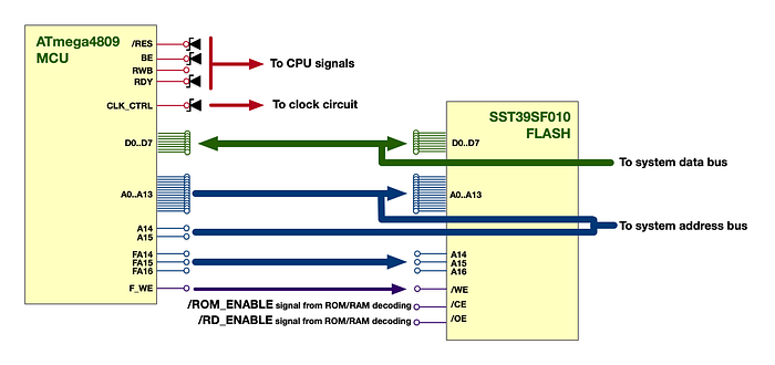
Signal summary
So, a quick recap of the signals managed by the MCU, plus some extras:
RDY: connected to the CPU, to stop it.BE: connected to the CPU, to release the buses andRWB.R/W: connected to theRWBline, to control decoding logic.CLK_CTRL: to stop thePHI2signal high.A14andA15: the top two bits of the address bus, used for decoding logic. These lines are not connected to the flash as that needs only address linesA0–A13as we're dealing in 16KB images.F_WE: This goes directly to the flash's/WEinput to enable write operations. There's a 3.3KΩ pull-up on this line.D0–D7: the system data bus.A0–A13: the lowest 14 lines of the address bus.FA14,FA15andFA16: These outputs go straight to the flash memory'sA14,A15andA16address pins to manage banking of the memory within the flash. There's no connection to the wider system.
Board design
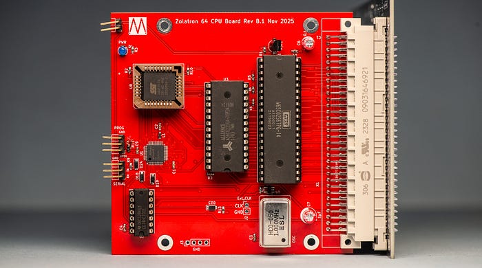
The board design posed no real challenges. In part, that was due to me having decided to use PCBWay's PCB Assembly service. The company had kindly offered to fab the boards for free to support this publication. The QFP version of the ATmega4809 is very small and I didn't fancy soldering it myself. That choice meant I could also opt to use other small surface-mount components, such as 0603 resistors and capacitors. In the end, there were acres of board space free (which might come in handy, as we'll see).
At the edge of the board are two serial connections. One is a standard UART-type connection for the MCU's serial port, so that it can talk to a remote computer. The other is a serial-based Unified Program and Debug Interface (UPDI) port for programming the MCU's own firmware.
Before the board arrived I knew I'd made a mistake. My playing around with AVR 0-series microcontrollers had made me dangerously confident about my grasp of the UPDI interface.
Long story short, I'd used a resistor where I should have used a diode. I also needed a pull-up that wasn't there.
Luckily, the fix was simple. I removed the resistor and replaced it with an SD103C Schottky diode. And I bodged on a 10KΩ resistor between the TX pin on the programming connection and the nearby VCC pin on the decoding chip. For safety, I wrapped the resistor and its legs in heat shrink.
It was a shame. Fresh from PCBWay the board looked immaculate. I just love the 'precision engineering' look of tiny components expertly mounted on the board. It makes it look as though I know what I'm doing.
There weren't that many SMD parts. Aside from the ATmega4809, they mostly consisted of resistors, bypass capacitors, diodes and NAND gates.
As with the other times I've used PCBWay's PCB Assembly service, the company sent me photographs of a prototype with the parts in place so I could check orientation of things like the MCU, other ICs and diodes, which is a great confidence booster.
Software overview
There's too much software to dissect it completely, but here's an overview.
Like I mentioned, there are two pieces of code that work together by passing instructions and data across a TTL serial connection. When the MCU gets a 'BURN' instruction from the remote machine, it:
- Pulls
BElow to tell the CPU to release the buses andRWB. The MCU subsequently takes control of these signals. - Pulls
RDYlow to stop the CPU. - Pulls
CLK_CTRLlow to stop thePHI2clock in a high state. - Sets
A14andA15which, via the decoding logic, asserts the system's\ROM_ENABLEsignal, enabling the flash chip. - Sets
FA14,FA15andFA16appropriately to select a bank within the flash memory. This is largely theoretical at the moment and something I'm working on.
The MCU then downloads the new firmware code in chunks and writes it straight to the flash memory. It manipulates the system-wide /READ_EN signal (connected to the flash chip's output enable, /OE input) by controlling the RWB signal. And it manages the flash chip's write enable (/WE) signal directly.
The code for all this is written in C++ and is available in the repository (make sure you look at the Dev branch).
On the dev machine side is a simple Python script (flashz.py) that talks to the MCU. This is designed to be called from a shell script that also assembles the ROM code. The code reads the whole 16KB ROM image into a single list (ie, array).
After the ROM code is sent, the MCU sends back the first 16 bytes which the Python code compares to the first 16 bytes in its array as a very basic check that the transfer was successful. That was how I knew it wasn't working.
Right time, wrong place
Once I'd eradicated the most obvious and stupid bugs in both sets of code I faced the daunting task of figuring out why the data seemed to transfer, but the check at the end always failed. Sometimes it would give all 0xFF values, which is what you'd expect from a freshly erased sector on the flash. Sometimes it was zeros.
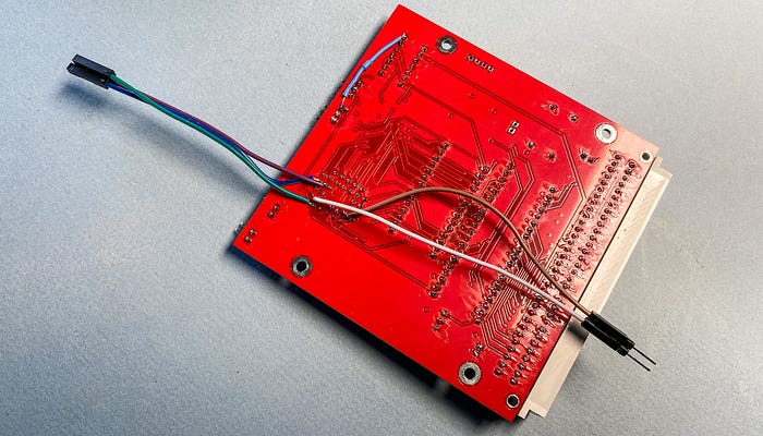
I soldered a couple of jumper wires to the flash's /OE and /CE signals (while cursing myself for not adding more test points to the board design). Then I hooked an oscilloscope or a logic analyser or an oscilloscope and a logic analyser to a wild variety of signals, all of which seemed to be doing exactly what they should be doing and in the right order. I was tearing my hair out (and I don't have much to spare).
Was it an error in my board design? Hours went by tracing every trace. Was in the logic in the MCU? Was the Python code doing something silly?
I was in that familiar place of 'it should work, so why doesn't it?'.
I'll save you the blow-by-blow. The tl;dr version of my struggle was that I wasn't handling the FA14, FA15 and FA16 signals properly. My focus was on setting A14and A15. But those are just for managing the decoding logic.
What I ended up doing, without knowing it, was writing code to higher parts of the flash's memory. It was getting there fine, but just to the wrong place.
Finally, everything was fixed. And it works a treat. In a sense.
Now, when I've finished making a change to the 6502 assembly, I invoke the build script from the command line. It builds the binary, saves it and uploads it via serial to the MCU on the Zolatron CPU board which copies the code to the flash memory and reboots the machine. The whole process takes a little under 14.5 seconds. And I can do all this from the sofa or the garden.
Crashing bore
Then I tried running 'Zumpus'. This is my version of the classic 'Hunt the Wumpus' text game. And I know that it works.
Except that now it doesn't. It runs for a while, stutters, tries to move on but eventually crashes. The same went for a short program I'd written to test maths functions.
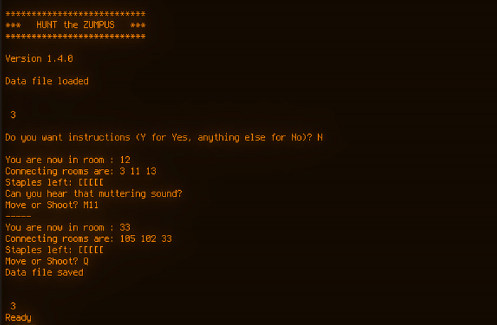
Okay, don't panic. As a sanity check, I replaced the new CPU board with the original EEPROM-based one, burned the latest version of the ROM code and tried these programs again. They crashed, albeit in slightly different ways.
And so a new prime suspect loomed into view. Me.
A few weeks ago I'd done a little, um, 'tidying up' of the code — mostly adding comments. But I did shift a couple of labels from one config file to another where they more logically belonged. These were names for memory addresses that I use a lot and which I reserve for special functions.
There were two in particular, called MATH_TMP_A and MATH_TMP_B and, as you might expect, these are memory locations reserved for holding temporary values during maths calculations.
Originally I had these configured to use locations in page 0 (RAM addresses $0000–$00FF). But zero page is a privileged area of memory with the 6502 and it's a sound idea to use it only for things that can benefit from those privileges (such as vectors). So I moved these memory locations to page 4 (addresses $0400–$04FF). But in doing so, I made a mistake. I reserved only one byte for each, but these are meant to be 16-bit locations.
Here's a section of the page 4 setup with the error in place.
EXTMEM_BANK = $0400 ; the first memory location label for page 4
TEST_VAL    = EXTMEM_BANK + 1
\ ... and so on, incrementing by the necessary number of byes each time...
RAND_SEED    = STR_BUF + STR_BUF_SZ   ; $042B 2B random seed number
MATH_TMP_A   = RAND_SEED + 2          ; $042D 2B
MATH_TMP_B   = MATH_TMP_A + 1         ; $042F 2B
UINT16_A     = MATH_TMP_B + 1         ; $0431 2B
In this case, MATH_TMP_A and MATH_TMP_Bare each one byte long. But my program code includes lines like this:
clc
lda MATH_TMP_A
adc MATH_TMP_B
sta FUNC_RES_L
lda MATH_TMP_A + 1
adc MATH_TMP_B + 1
sta FUNC_RES_H
This is 16-bit addition. See the problem? I'm referring to locations such as MATH_TMP_A + 1 which I'm using to store the high byte of a 16-byte value. But in the way I had things configured, MATH_TMP_A + 1 was the same as MATH_TMP_B. My values were stomping on each other. Oops.
Fixing it was a matter of doing this:
EXTMEM_BANK = $0400 ; the first memory location label for page 4
TEST_VAL    = EXTMEM_BANK + 1
\ ... and so on, incrementing by the necessary number of byes each time...
RAND_SEED    = STR_BUF + STR_BUF_SZ   ; $042B 2B random seed number
MATH_TMP_A   = RAND_SEED + 2          ; $042D 2B
MATH_TMP_B   = MATH_TMP_A + 2         ; $042F 2B
UINT16_A     = MATH_TMP_B + 2         ; $0431 2B
That makes MATH_TMP_A and MATH_TMP_B two-byte locations. I also found a bug in one maths routine, a 16-bit addition.
All the program crashing went away. At least on the EEPROM-based machine.
Too fast to live?
With the flash-board CPU swapped back in, things started crashing again. Simple programs would work. Most of the operating system commands worked. But Zumpus and that maths program were deeply uphappy.
And that's when I started worrying whether the flash memory is just too good.
The AT28C256 EEPROMs I've been using have a 150ns read access time. With the SST39SF010 flash, the maximum access time is 55ns. I thought this would be a good thing.
To give you a hint as to the level of my desperation, I must now confess that I turned to AI for help. I asked Perplexity: "With a 1MHz 8-bit computer, is it possible for the ROM to be too fast?"
Its answer was detailed but can be summarised as: "You betcha!"
It's not about getting valid data on to the bus — a faster speed is an asset there. But the response touched on areas such as the ROM reacting to transient bus or control signal glitches, timing issues that were maybe a bit marginal and are now problematic, and more.
If you've got any thoughts about this I'd be glad to hear them.
I'm going to delve into this in more detail in a future article where I'll take Perplexity's advice and crack out the oscilloscope and logic analyser again. In the meantime, I'm playing around with two copies of the Zolatron — one with EEPROM and the other with flash.
The concept works, and in many ways works well. But when combined with my naive, self-taught approach to electronics, it's not being given a fair chance. More on that soon.
You can find all the stories related to this project on the Zolatron feature page.
There is also a GitHub Zolatron repo with the code, datasheets and other documents.
Many thanks to PCBWay for supporting this publication by supplying free PCBs and assembly.
Steve Mansfield-Devine is a freelance writer, tech journalist and photographer. You can find photography portfolio at Zolachrome, buy his books and e-books, or follow him on Bluesky or Mastodon.
I'm also posting these articles on Substack, where you'll find additional articles, notes, updates, asides and chats. Subscribe there for the most complete experience.
Or you can buy Steve a coffee — it helps keep these projects going.