RETROCOMPUTING
In three previous articles we looked at programming flash chips, creating a development board for experiments and the software to use it. Which was all a lot of fun. But I'm starting to think it was heading in the wrong direction.
The purpose of the Flash-based ROM project was to come up with an alternative to using EEPROMs in my the Zolatron 6502-based homebrew computer.
In this article, we'll look at some other ideas — three of them, to be precise — to how we might employ flash memory to act as a ROM in a homebrew computer. This documents my thought process, which slowly evolved to a point where smarter people might have started.
The problem
The ROM code is a critical part of the system as it contains the software to boot the machine and provide key operating system functionality.
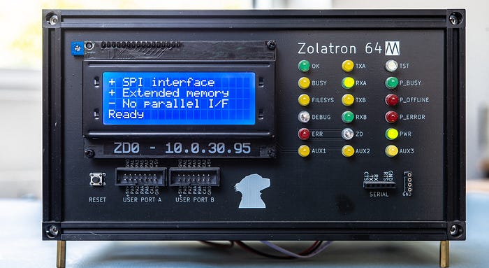
And for the sake of clarity, let me emphasise that whenever I say 'ROM' here I usually mean something fulfilling the role of read-only memory. So far with the Zolatron this has consisted of an AT28C256 EEPROM.
I program this by flashing the binary code to the EEPROM with a USB programmer device. So each time I make a change to the ROM code I have to perform the following ritual:
- Switch off the Zolatron.
- Remove the EEPROM from the ZIF socket and insert it into the programmer.
- Run a script on the dev PC to assemble and flash the code to the EEPROM.
- Watch with dismay as the script reports a verification failure.
- Re-seat the EEPROM in the programmer.
- Run the script again.
- Remove the chip from the programmer and insert it into the Zolatron.
- Switch on the Zolatron.
This is a long list (even if the flashing of the code works the first time). Worse, because of how things are laid out in my office, it involves me getting out of my chair. Twice!
In situ
That's more exercise than I want at my age. And there's always the possibility — or perhaps inevitability — that my changes to the code have introduced a bug and I'll have to do it all over again minutes later. That's why I started thinking about using flash memory in place of the EEPROM, so that I could program it in situ. Basically, I want to reduce all of the steps above to just one — the build script. There should be no manual intervention — no removing chips, flipping switches, pressing buttons or attaching wires.
Having discussed this on forums I received a bunch of suggestions. These included getting the 6502 itself to handle programming the flash, running everything from RAM, using the dev PC itself as the ROM, feeding ROM data to the Zolatron over serial, and more.
But many of the suggestions had downsides or their own complexities, such as having to always have the dev PC attached, writing boot loaders or doing many other clever things that are outside my comfort zone. I do believe in stretching oneself, but there are only so many learning curves you can climb at once. Besides which, I had already started down a particular road and wanted to see where it led me.
Too many pieces
The approach I adopted in the previous articles seemed simple enough. A microcontroller (MCU) on the Zolatron talks via serial to the dev PC and responds to commands. The dev PC pushes the new ROM code to the MCU which stores it temporarily in RAM and then, on another command from the PC, writes the code from the RAM to the flash chip.
And this process works. My dev board and code proved the concept. But if you're thinking that it sounds a tad clumsy, you're not wrong.
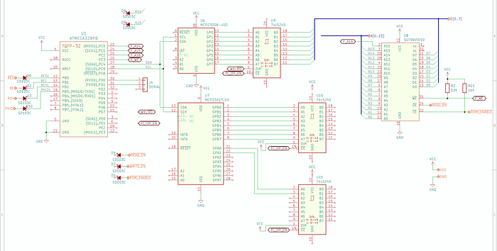
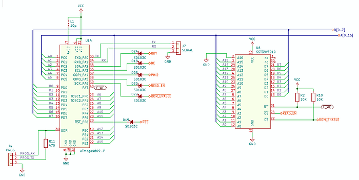
For one thing, this original approach demanded some extra chips. I'd chosen the Microchip ATmega328PB as the MCU because it's small and I'm very familiar with it. But it doesn't have enough GPIO pins to accommodate the 8-bit data bus, 16-bit address bus and the various control signals we need.
The solution was to use two I2C-controlled port expander chips, an 8-bit MCP23008 for the data bus and a 16-bit MCP23017 for the address bus. This is what I'm using on the development board.
So that's five chips (MCU, RAM, flash and port expanders) to replace one (the EEPROM). Unlike the development board, when the time comes to implement to concept on the computer we don't need the RAM — the Zolatron already has enough for our purposes and we can borrow that. But when I tried designing a new version of the Zolatron's CPU board to incorporate these ideas, I ran into another problem.
Yet more chips
The outputs of the port expanders are connected directly to the data and address buses. However, after flashing the new code, they need to disconnect. Alas, there seems to be no way of putting the outputs into a high-impedance (high-Z) state.
And so I introduced 74HCT245 transceiver chips. These can set their outputs to high-Z. But I needed three of them to buffer both the address and data buses.
Compared to the original CPU and memory board of the Zolatron, we now have six extra chips. That's not good.
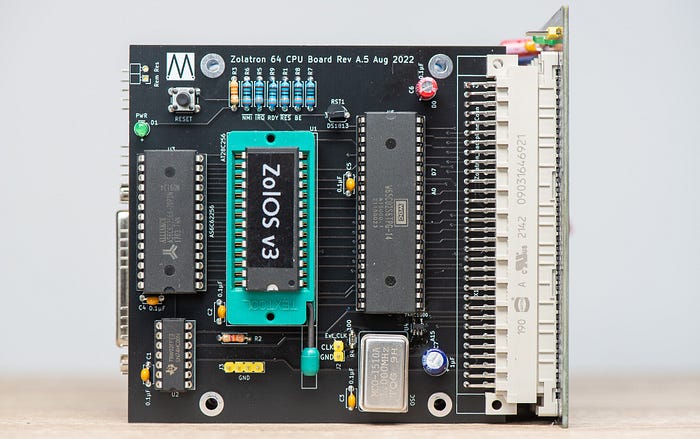
This is how it was starting to look in the schematic. This is just for the 'flash ROM' section of the CPU board — it doesn't include the CPU itself, RAM, oscillator, decoding etc.
Don't try to build this. The schematic is incomplete because I ran out of enthusiasm for this approach.
A better MCU
Why not use a larger MCU with more GPIOs and cut out the port expanders and transceivers entirely? Good idea.
Casting around, I looked briefly at STM microcontrollers, but decided I didn't want to learn a whole new toolchain. Remaining within the Microchip AVR family would be a simpler transition.
And so I settled on the ATmega4809, one of the relatively new family of 0-series (or AVR0) chips introduced in 2016. This comes in several flavours but I focused on two — the -P model which is available in a 40-pin DIP package and the 48-pin TQFP-format -A device. Both have internal oscillators running by default at 20MHz, so a slight speed boost over the ATmega328PB (and no need for an external crystal and capacitors).
The -P model is slightly disadvantaged compared to the -A in that it has fewer GPIOs, and this will turn out to be significant.
Another plus point is that the chips are programmed via a single, dedicated UDPI pin. I'll be writing an article about UPDI programming soon.
And … the ATmega4809 has 32KB of flash memory, which is enough to hold the necessary code and an entire 16KB ROM image. We'll be getting to that.
Via RAM
Going back to the original idea of using RAM as an intermediate step, the first step was to check whether the DIP version of the microcontroller had enough pins to do the job. There are a lot of signals we need to accommodate.
The data and address buses take up 24.
Next, with the overall goal of integrating the solution into the Zolatron's CPU board, we need to consider the environment we're operating it. I don't want to have to power down the Zolatron in order to rewrite its ROM, and that means the clock will be ticking, the CPU will be asserting values on the address bus and various chips (including the CPU) will be messing with the data bus.
The solution is to exploit the 65C02's Bus Enable (BE) and Ready (RDY) signals low to put the CPU into a passive state. We'll cover this in more detail in the next section, but for the time being just accept that we need these signals.
However, if the clock is still ticking, the Zolatron's decoding logic is likely to be having some effect on critical signals — notably ROM Enable (/ROM_ENABLE), Write Enable (/WRITE_EN) and Read Enable (/READ_EN).
My first instinct was to try pulling these lines and the PHI2 clock low with one MCU pin, via a diode, but this is a bad idea. Two of these signals have pull-ups and the poor MCU pin might get overloaded with current. So we need even more pins. (And, as it happens, these weren't good ideas anyway.)
Two pins are spoken for by the serial port to connect with the dev PC. The MCU also needs to be able to pull the control signals I mentioned earlier low:
/READ_EN, to be able to read from RAM and flash./WRITE_EN, to be able to write to RAM./ROM_ENABLE, to enable the flash chip.
And we have to be able to strobe the system /RESET line low to reboot after flashing.
We need at least one more signal attached to the flash chip to pull its /WE (Write Enable) pin low. Why not use the system's R/W signal? Because that's attached to the RAM too. Things could get messy.
Finally, I'd like to be able to control the flash chip's A16pin (we already need to control A15 when writing to and reading from RAM). This would give us the option of writing ROM images to other banks within the flash, created a multi-ROM solution. This isn't something I've explored much yet, but the option would be nice.
How many pins is that? I've lost count but it was clearly becoming a problem. That goes away if we use the ATmega4809-A instead, with its extra GPIOs. We'll get into that later, though, because I'd started to lose interest in the RAM-oriented idea and we do have some other options to consider.
Direct to flash
One possibility is for the MCU to write to the flash directly, cutting out the RAM. This would speed things up. It would require some clever flow control in the code, but what's life without a challenge?
This approach relieves us of the need to handle /WRITE_ENbecause we're not messing with the RAM. If we ignore the A16 signal (pulling it permanently low on the flash chip) the DIP version of the ATmega4809 becomes a possibility.
To try this out, I first modified the code I'd been using with my dev board. If you look at the GitHub repository for this project, you'll find a number of programs. The flashprog program is ATmega328PB code to run on the dev board while flashterm.py is Python code for the dev PC that allows us to talk to the dev board. I updated both to add an option to load ROM code directly to the flash without passing through RAM. It works, taking about 1m 45s. So the idea is sound.
New code
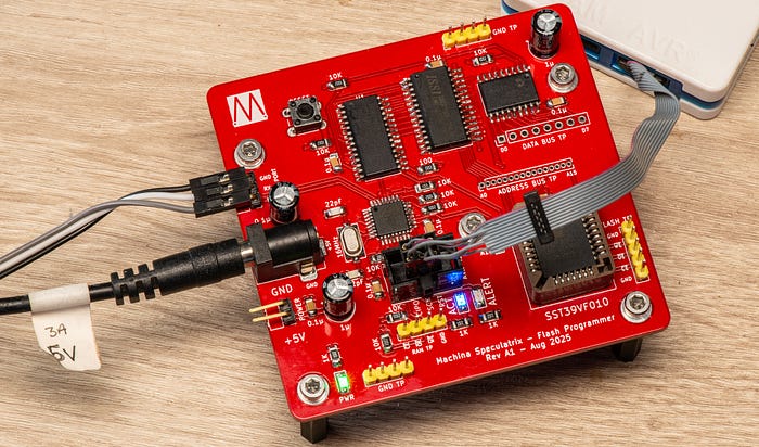
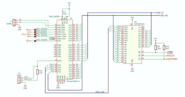
Next, I built a prototype with the ATmega4809-P on a breadboard and my breakout board for the SST39SF010 flash chip. This required new code.
I created ATmega4809 firmware called flashz and a corresponding Python program (flashburn.py) that does away with the niceties of Curses found in the flashterm.py. Instead it simply gets on with pushing the ROM code to the MCU which writes it, 64 bytes at a time, to the flash chip. The Python program is designed to run silently by default, for use in build scripts, but a verbose option is available.
I also built in options to erase the flash chip (at least, the lower 64KB), and to read back 256 bytes from a given start address (again, within the 64KB address space).
Upload and flashing of a 16KB image took 27 seconds at 9600 baud. After boosting the serial speed to 38400 baud, that dropped to a little under 13 seconds. The limiting speed is the time taken to write to the flash, so increasing the baud rate further is unlikely to bring significant benefits. And it's still an awful lot faster than the process involving removing, burning and replacing EEPROMs.
In circuit
So the idea is basically workable. However, all we were doing with the prototype was pushing code to a flash chip that wasn't connected to anything but the microcontroller. In the Zolatron, we'll be faced with a significantly different environment.
The 'ROM' in the Zolatron is also connected to the system-wide /READ_EN signal and a /ROM_ENABLE signal. Also, the computer will be running, so the CPU will be putting values on to the address bus and several devices might be doing unspeakable things with the data bus. This would be highly disruptive to our attempts to burn the new ROM image into the flash. And the clock (PHI2) will be bouncing up and down.
The solution is to stop the clock and CPU, allowing the microcontroller to assume control of all the important signals. This is entirely feasible by pulling the CPU's BE and RDY signals low and adding some extra logic to the clock generator.
After a lot of false starts and having my ideas rejected and corrected by fellow 6502.org forum members, I have what I think is a workable plan.
However, I still need to test the idea and, ideally, respin the main CPU PCB for the Zolatron to find out if it really works.
I've started work on a new CPU board design. Routing all the signals on the PCB is turning out to be non-trivial, so it's a work in process. I'll save all the gory details for a future article that will cover both the prototype and PCB and will go into full detail about how the microcontroller takes command of all the important system signals and decoding inputs.
MCU as ROM
Finally, and most radically, we can do away with the flash chip altogether. Yes, I know these articles are all about using flash in place of ROM, but bear with me. We'll still be doing that, but in a simpler fashion.
Like most microcontrollers, the ATmega4809 stores its program in flash memory. You can also put immutable data there.
So why not do away with the flash chip, put the ROM code in the MCU's flash memory and just have the microcontroller run a program to serve up data as if it were a ROM?
One possible objection is speed. We're going to have to write code for the MCU to respond to signals from the CPU and set the data bus accordingly. If you're one of those people who likes to push the 65C02 to silly speeds, that's going to be a problem. But I'm not one of those people and an ATmega4809 zipping along at 20MHz is perfectly fast enough to behave like a ROM as far as the 1MHz Zolatron is concerned.
It will require some clever assembling of the code. My aim is to have a single Bash script that assembles the 6502 code into a binary ROM image, then runs a Makefile for the ATmega4809 code that creates an object file from this binary and, when building the AVR code, links to that object file. In this way, the ROM code is integrated into the AVR's program code and gets written to the MCU's flash memory.
When the MCU reboots and behaves like a ROM, it watches for the /ROM_ENABLE line to go low, reads the address bus and outputs the relevant data byte.
Aside from the data and address bus lines, the MCU just needs to connect to /ROM_ENABLE, /READ_EN and /RESET. No serial port required. When the /ROM_ENABLE is high (ie, the computer is not addressing the ROM), the MCU sets all the pins for the data and address buses to inputs, which puts them in a high-Z state.
The DIP version of the MCU is perfectly capable of handling this, which should allow me to prototype the concept. However, for the final thing, I'll use the TQFP package which should allow me to create a board roughly the same footprint as the EEPROM chip.
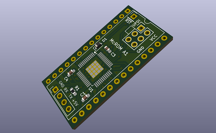
As it's a microcontroller-based 'ROM', I'm calling this project the McROM. (Be grateful I didn't call it 'Rommy McROMface'.) Code for this is going to be in the Zolatron repository.
Seems like the easiest solution, no? Why didn't I start with this? Another good question. Answers on a postcard, please.
The one possible downside is that we'll almost certainly need to switch off the Zolatron while flashing new code to the microcontroller. That's something that needs to be explored.
Future plans
For the sake of science, and to appease my curiosity, I plan to explore all these options. The roadmap looks something like this:
- Respin the PCB for the Zolatron CPU board with an ATmega4809-A (the TQFP version) and flash chip.
- Create a PCB that has an ATmega4809-A with programming header pins and signals broken out in such a way that the board will simply drop into the socket intended for the AT28C256 EEPROM. As you saw above, I already have a design for this.
There will be full articles on these experiments, and updates in the Lab Notes newsletter.
I'm also planning related articles soon on:
- Programming AVR chips via UDPI, instead of the more common ISP.
- Incorporating binary code into your AVR program.
Stay tuned.
There's a GitHub repo for this flash programmer project, which includes schematics and Gerbers for the PCB, C++ code for the ATMEGA328PB and Python code for the PC.
The articles relevant to this project are:
- Using flash memory as a homebrew computer ROM.
- A development board for flash-based ROM.
- Software for the flash ROM development board.
- Alternatives to ROM for a homebrew computer (this article).
Steve Mansfield-Devine is a freelance writer, tech journalist and photographer. You can find photography portfolio at Zolachrome, buy his books and e-books, or follow him on Bluesky or Mastodon.
Sign up for the Machina Speculatrix Lab Notes newsletter.
You can also buy Steve a coffee — it helps keep these projects going.