ELECTRONICS
Not all chips are breadboard-friendly. Indeed, we're seeing a trend towards an ever-higher percentage of ICs being available only in surface-mount packages. If you're lucky, that might mean something relatively easy to hand solder, such as SOIC formats. But the various forms of quad flat package (QFP) can be difficult for the homelab bodger, like me.
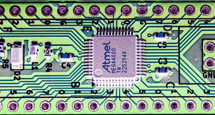
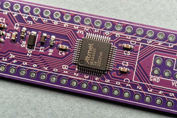
Which was a problem when I decided I needed to use the ATmega4809 microntroller.
Sure, it's available in a DIP-40 format, which uses the same die as the 48-pin TQFP version. But it sacrifices eight GPIO pins. Like phantom limbs, you can't just ignore those missing pins. The datasheet advises: "the pins PB[5:0] and PC[7:6] must be disabled (INPUT_DISABLE) or enable pull-ups (PULLUPEN)."
I don't know about you, but when I have a microcontroller I want access to all its capabilities. I selected the ATmega4809 precisely because of that high GPIO count. Besides, a 40-pin DIP chip is big.
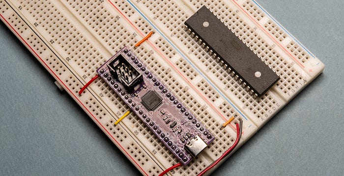
The immediate solution to this conundrum was to buy both DIP and TQFP versions, using the DIP chip on breadboard prototypes but with a view to targeting its physically smaller sibling in code.
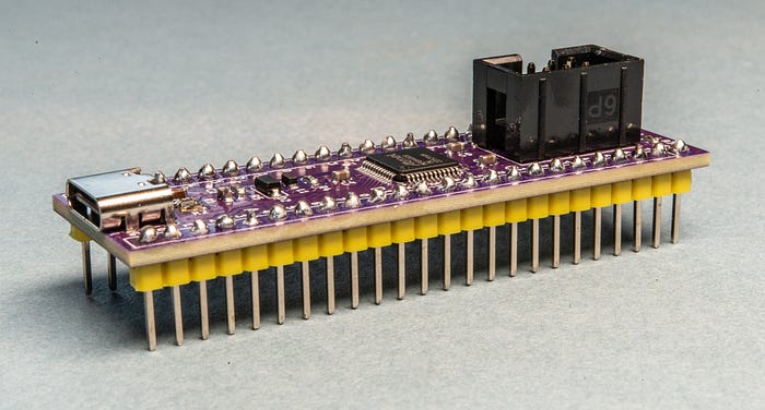
But that's still a compromise. I really wanted to be able to experiment with the fully fledged version of the ATmega4809. Which is why I came up with a dev board, which turns the TQFP version of the microcontroller into a 48-pin DIP.
All the things
Arguably, it's more of a breakout board than a dev board, because it doesn't do a lot more than break out the chip's pins to headers. But there some quality of life additions.
You can buy ready-made TQFP breakout boards. Just solder on the chip and you're done. Of course, soldering on the chip is the problem.
You can also find reasonably priced zero insertion force (ZIF) sockets for TQFPs which convert them to bizarrely wide DIP arrangements that aren't entirely breadboard friendly. But all these boards do is break out the pins. I wanted something just a little more supportive.
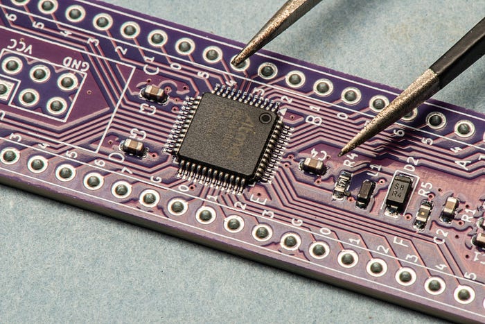
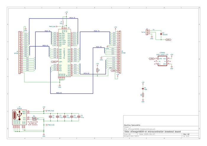
For a start, I figured it would be useful to have onboard decoupling capacitors for the chip's power pins. I put them near the pins themselves and also across the power input to the board.
As for power, you can provide it via the power pins on the header rows (there are VCC and GND pins at the ends of each row) or through a USB-C socket. The socket is wired purely for power, with the CC1 and CC2 pins pulled low via 5.1KΩ resistors.
One compromise I made was to connect AVCC (the voltage supply for analogue pins) to VCC, via a 10µH inductor. This means I can't use a separate VCC reference voltage for analogue stuff, which is fine by me because I'm mostly interested in digital signals. Maybe I could break this out separately on a version B, with a jumper to give you the choice. But that's for the future.
The board has a power LED to tell you the electrons are flowing. I always find that comforting.
However, the key convenience feature I built in was concerned with programming. And this is where I made my main mistake.
Programming pins
On AVR 0-series boards, you program the chips via the single Unified Program and Debug Interface (UPDI) pin. However, there's a bit more to the connections than a single wire.
One programming option is to use a USB-to-serial cable. In theory, you can just connect the TX pin of the serial cable to the UPDI pin of the microcontroller. In practice, it's a little more complicated. And it can become a lot more complicated if you're not paying attention (note to self).
One common solution you'll see touted widely on the interwebz is to connect the TX pin of the serial cable to UPDI via a 470Ω resistor and the RX line directly to UPDI (see the diagram lower down). And whatever solution you use, you'll want a common ground connection between the serial cable and the microcontroller.
And I swear I got this arrangement working for a while. But when I came back to it some time later there was no magical incantation I could use to get the setup to function.
Protective diode
Greybeards on the internet suggest a Schottky diode for protection, and there are all sorts of permutations employing resistors at various locations. The most exhaustive explanation I've found is here, but you can drive yourself a little mad trying to optimise this, and I think that's what happened to me.
For the original version of the board, which I had fabbed, I included a diode and a resistor. But I'm pretty sure the diode is the wrong way around. In any case, the chip simply ignored my attempts to program it via serial. (We'll come back to this later.) Luckily, I also included an alternative.
If you have an Atmet-ICE programmer — which I'm glad to say I do — then you can forget all about the complications of resistors and diodes. You use the same cable between the Atmel-ICE and the board that you are familiar with when accessing the six-pin In-Circuit Serial Programming (ICSP) headers often found on ATmega (older series) microcontroller boards, including many Arduinos. The 2x3 arrangement of pins carry VCC (as a programming reference voltage, not to power the board, which needs to be powered separately), ground, a reset line and the three signals associated with the SPI interface — COPI, CIPO and SCK (they are often known by other names).
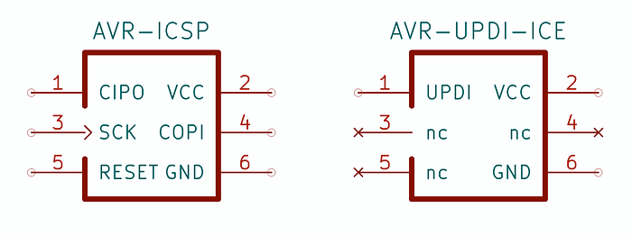
In the UPDI context, three of the pins are unused and pin 1 (which was Controller In Peripheral Out, aka MISO) becomes the UPDI pin. But you don't need to worry too much about the details. Just plug in the cable from the Atmel-ICE, tell your Makefile or software that you're using the atmelice_updi as a programmer and it just works.
(Incidentally, I'll have another article coming soon that will go into more detail about programming AVR0 devices via UPDI.)
Designing the board
Routing the board layout wasn't that difficult, although please be aware that the design you see in the diagrams and schematic are not the same board as the one in the photographs. I have since revised the design in light of my mistakes.
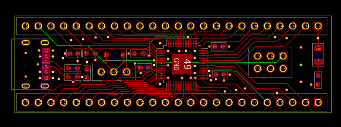
The board's pins span the same width as a standard 15.24mm wide IC — ie, the same as the DIP-40 version of the microcontroller — although it's significantly longer.
The datasheet notes: "The center pad underneath the QFN packages can be connected to PCB ground or left electrically unconnected. Solder or glue it to the board to ensure good mechanical stability."
I chose to connect it to ground and while I left the pad free of vias, there are several ground-stitching vias around it. This, by the way, is a four-layer board with internal VCC and GND planes.
For the passives, I went with 0603 (imperial, 1608 metric) SMD parts in order to save as much space as possible. I knew this was going to be a tight fit.
Cramming it all in
In fact, the most difficult job was getting everything I needed on the silkscreen layers. I wanted all of the pins to be labelled on the top. I strongly dislike having to constantly refer to a datasheet to work out where to connect my wires.
With some pins there was enough space, but many were heavily constrained. I opted for the tactic of using just a number next to the pin. So, for example, pin PB3 is just marked Ɖ'. But I also put the port name — A, B, C, D, E and F — somewhere nearby.
Other pins were also abbreviated — + for VCC, G for ground, U for UPDI and /R for reset/PF6.
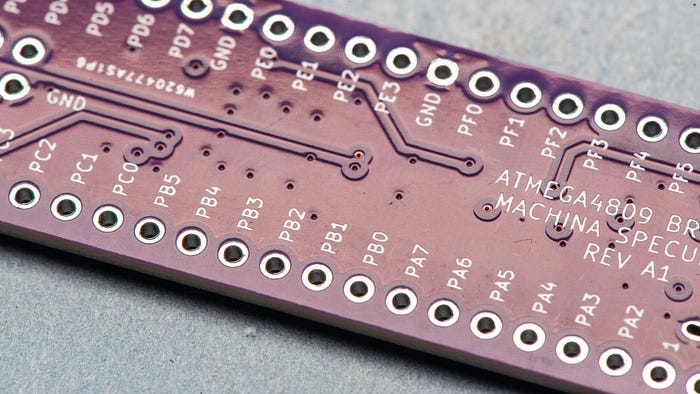
I also labelled the pins on the back of the board, but more completely here — 'PB3', for example.
Even using abbreviations, I found myself using the smallest text size I thought I could get away with. PCBWay recommends a minimum size of 0.8mm and thickness of 0.15mm, and that's the size I used for a lot of the labelling. However, in some cases I broke the rules and went for 0.1mm thickness. I was intrigued, and nervous, to see how that would work out.
Pin 40 on the chip, aka PF6, doubles as an active-low reset signal, so there's a 10KΩ pullup resistor (R5) on that to prevent it going off by accident. By default, the ATmega4809 has this pin set for use as a GPIO, so that pull-up might not be needed. You can always desolder it. To get pin 40 to act as a reset signal, you need to change a fuse.
A fab job
I mentioned PCBWay because the company had kindly offered to manufacture the board for free — and that included offering its PCB assembly service to both source and solder the surface-mount parts.
When the boards, in a charming shade of purple, arrived, I was glad I'd gone for this option, especially when I saw just how tiny, and close together, the pins of the ATmega4809 are. Plus, those 0603 parts are like grains of rice.
The board looks beautiful (in my eyes). Everything is precisely put together. It somehow makes me look far more professional than I am. And that includes the silkscreening. Even when pushing beyond the recommended limits, the text is crisp and readable. (Well, okay, my old eyes do need a bit of help from a magnifying glass, but that's just me.)
Fixing the errors
Obviously I needed to revamp the design a bit.
When the time came to solder the USB-C connector I found that I'd made life difficult for myself. There's a row of two resistors and one capacitor that are much too close to the socket's pads for comfort. I got the pins soldered, but how well I'm not sure. In the revised design I've left a lot more space.
The only thing that wasn't working on the board was serial programming via the UPDI header pin. Programming with the Atmel-ICE via the ICSP socket works just fine, so the boards are entirely usable. But that error bugged me.
I went back to the breadboard to see if I could solve the issue. I thought it might have something to do with my USB-to-serial cables. There can be significant differences between adapters according to which chip they use — FT232, CH340, PL2303 etc — and also whether the chips are genuine or knock-offs.
I have two types of USB-to-serial cable based on the FT232 and PL2303. Both refused to work. Then I looked again at the wiring and thought about how those greybeards insist on a diode. I replaced the resistor with an SD103C Schottky diode and voilà, it worked.
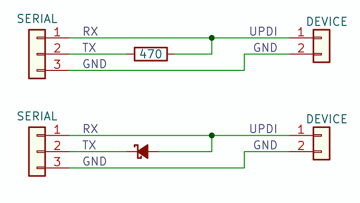
In the diagram above, note the orientation of the diode. This looks all kinds of wrong to me, but it does work. Maybe someone could explain it to me. [EDIT: I've found that a weak pull-up resistor — say, 10KΩ — between the UPDI line and VCC makes for a more reliable connection, at least with the USB-to-serial cables I'm using. Your mileage may vary.]
Anyway, in the revised design, I did away with the resistor and turned around the diode. Then I added a three-pin header for use with serial cables. You connect the serial's RX line to the UPDI pin, the TX to TX and ground to GND.
I don't know yet whether I'll order copies of the revised design, but I do plan to make it available via PCBWay's Shared Projects platform.
For now, I'm having too much fun playing with my new board.
Many thanks to PCBWay for supporting this project by supplying free PCBs and assembly.
Steve Mansfield-Devine is a freelance writer, tech journalist and photographer. You can find photography portfolio at Zolachrome, buy his books and e-books, or follow him on Bluesky or Mastodon.
I'm also posting these articles on Substack, where you'll find additional articles, notes, updates, asides and chats. Subscribe there for the most complete experience.
Or you can buy Steve a coffee — it helps keep these projects going.