RETROCOMPUTING
The chips on your homebrew computer need to talk to each other. How do they do this? They take the bus.
Buses are used frequently in electronics and there's nothing particularly special about them. A bus is simply a number of connections (wires, if you like) that are grouped together to achieve a common purpose.
Catching the bus
On the Zolatron, as with most simple 8-bit computers, there are two buses we care most about — the data bus and the address bus. The purpose of each is to carry a numerical value from one chip to at least one other. This is coded in binary, with each wire carrying a 1 (high voltage) or a 0 (low voltage).
I say 'at least' because the value of using a bus is that you can attach multiple devices to it, all of which share a common data path. Which chip actually uses the information on the bus at any given time is the subject of this article. But before we get into that, let's take a quick look at the two buses we'll be taking. (I'm overworking this bus metaphor, so I'll stop now.)
One thing to keep in mind is that the CPU — the humble 65C02 in the Zolatron's case — is at the core of all this, as the word 'central' in the CPU acronym suggests.
Data bus
On the Zolatron, the data bus is eight bits wide. This means it can carry numeric values from 00000000 to 11111111in binary. That's 0–255 in decimal or $00 to $FF if you prefer hexadecimal. (Using $ to denote hex is how we rolled in the 80s — none of that 0x nonsense.) It's also exactly one byte.
The data bus allows the CPU to either read a byte of data from a device (such as memory, a serial interface or whatever) or write a byte to it. In other words, it's a two way street. Which way it's going is determined by the CPU and your code. The pins on the CPU (and on peripheral devices) that connect to the eight wires of the data bus are usually designated D0–D7 (although you may encounter other labels — the RAM chip shown below uses DQ0–DQ7).
Address bus
The 65C02's address bus is twice as wide — 16 bits. This means it can carry values 00000000 00000000 to 11111111 11111111, or 0–65,535 or $0000–$FFFF. Note that 65,535: given that 1K is 1024 bits, the maximum number on the address bus is 64K. And we use this to 'map' our address space, so that with a 16-bit address bus we can address (designate) 64K individual locations. The pins/signals are usually labelled A0–A15.
It works like this. If the CPU wants to write a byte to a device, it puts the device's address on the address bus by setting its pins high or low appropriately, and it puts the byte's value on the data bus in the same manner.
Reading a byte from a device is a similar process. The CPU puts the device's address on the address bus and reads whatever the device has put on the data bus.
There's a little more to it than that, involving pins on the CPU that enable write or read modes, and the system clock. But that's the basic principle.
Talk to me
So how does a particular device know it needs to read or write to the data bus? Or how does the CPU select the device it wants to read from or write to? That's where address decoding comes in. And we'll start with a very simple example which, in the case of the Zolatron, is the RAM.
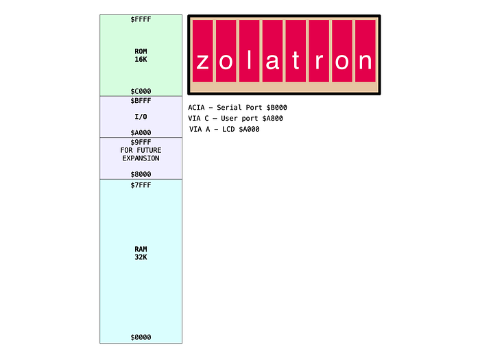
In the Zolatron's basic address map, the 32KB of RAM sits at the bottom — addresses from $0000 to $7FFF. (I'm going to use hex from here on.) It occupies not one address but 32K of them. Each memory location in the RAM gets its own address. So any time the CPU sets an address in that range, the RAM chip needs to know, 'oh, it's talking to me'.
Luckily, all the chips that we care about when discussing addressing have a handy pin. Typically, this is known as /CE for 'chip enable'. (Again, you may encounter other terms, but this is the most common and the one we'll use.)
On datasheets you'll normally see it with a bar drawn over the top, or possibly with a hash mark (I'm using a slash because it's easier). This means it's 'active low'. The chip is enabled when the signal going to the pin is in a low state (0V). If the pin is in a high state (5V on the Zolatron), the chip is disabled and ignores whatever is happening on the buses.
This is the pinout AS6C62256A 32KB SRAM chip I'm using in the Zolatron.
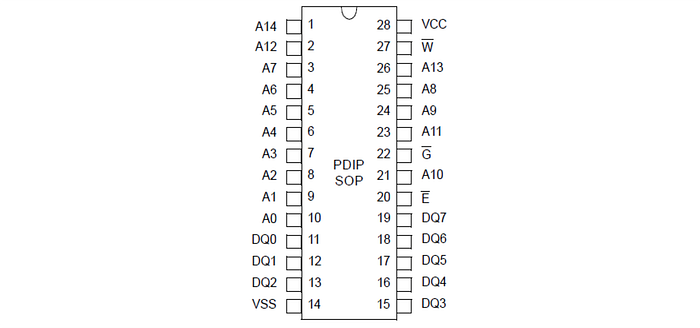
The chip enable pin is number 20 and is just labelled /E here, but it really means /CE. There are two other active-low pins that will play a part and these could be connected directly to the CPU (although we'll get to why we don't in a moment). The /W pin (more commonly labelled /WE for 'write enable') is an input that, when pulled low, tells the RAM chip that the CPU wants to write to it. The /G pin (usually known as /OE for 'output enable') is an input that is pulled low to tell the RAM chip to put the contents of the memory location specified by the address bus on to the data bus.
Active pins
There's something interesting going on here which is best understood by looking at all the pins of the address bus.
To help us along, here's a little table of the values associated with the address pins of the 6502 when each is set high.
PIN  HEX    DECIMAL
A0   $0001       1
A1   $0002       2
A2   $0004       4
A3   $0008       8
A4   $0010      16
A5   $0020      32
A6   $0040      64
A7   $0080     128
A8   $0100     256
A9   $0200     512
A10  $0400    1024
A11  $0800    2048
A12  $1000    4096
A13  $2000    8192
A14  $4000   16384
A15  $8000   32768
Note how A15 represents a value of $8000. But all the RAM addresses are below that. The highest is $7FFF. The 32K addresses of the RAM chip use only A0–A14 of the address bus. Put another way, 32K is addressable with 15 bits. The 16th bit (A15) is never used and is always set low whenever we want to address RAM.
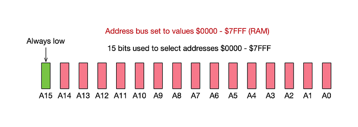
Conversely, whenever we want to address anything in the address map above RAM, A15 is always automatically set high because all the address values are at least $8000.
Remember how the 'enable' (/CE) pin of the RAM chip is active low? All we need do is connect A15 to the enable pin. When we set a RAM address on the address bus, A15 will be low and the RAM will be enabled. Whenever the CPU talks to devices at higher addresses, A15 will be high and the RAM will be disabled.
With that one simple step, we have 'decoded' the RAM addresses. And it will work. Sometimes.
Clocking in
There's a slight problem with this design. The RAM chip does its stuff when the /CE (chip enable), /OE (output enable) and /WE (write enable) lines are set in the appropriate states. But unlike many of the other major chips you'll find in the computer's design, it doesn't wait for the starting gun signal of the system clock transitioning from low to high before doing its work. In fact, the RAM chip has no clock pin.
This can lead to problems. The 6502 CPU might still be in the process of sorting out the address lines at the moment those other lines are set. This could lead to data being written to the wrong address. (Reading is less critical because that's more under the control of the CPU.) Basically, the rule is that you should never perform a RAM operation when the 6502's clock is low — only when it has gone high.
At a slow clock speed (like the 1MHz of the Zolatron) you might get away with this. And I did for quite a while on the breadboard prototype. All the same, it's good practice to ensure that things happen only when they should.
Send in the NAND
The solution for me was to use that most versatile of all logic gates — NAND. This is the inverted version of the AND gate. In the latter, the output is true (ie, 1) if, and only if, both of the inputs are true. All other conditions produce a 0 output.
The NAND gate inverts this so that the output is 1 unless both inputs are 1. This is the truth table:
Inputs | Output
A | B | Y
-------+-------+--------
0 | 0 | 1
0 | 1 | 1
1 | 0 | 1
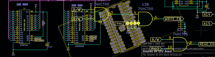
1 | 1 | 0I used a 74HCT00 chip which boasts four NAND gates. But I didn't use it with the A15 line — that's still connected directly to the RAM chip's /CE pin. Instead, I chose to 'qualify' the /WE and /CE signals going to the chip.
The 65C02 has a R/W output. This is often spoken as 'read not write'. The signal goes high when the CPU is performing a read operation. It goes low when doing a write. But the RAM chip doesn't have separate pins for read and write operations.
So here's how this works.
Read/write
We connect the R/W signal from the CPU to both inputs of one NAND gate. This is a simple way of just inverting the signal. When R/W is high, the NAND gate's output is low and vice versa.
We then feed that output into one of the inputs of a second NAND gate. The other input is connected to the CPU's PHI2 clock output (which is the clock signal for the whole machine).
The result is that the output from this second NAND is low when (and only when) both the PHI2 is high and R/W is low — ie, signalling a write. The 'write' signal from the CPU is 'qualified' or 'gated' by the clock, so that it's active (remember, it's 'active low') only when the clock is in the appropriate state — ie, high. I called the output signal from this second gate /WRITE_EN (for 'write enable'). And I connected this to the RAM's /WE pin.
Similarly, I connected PHI2 and R/W from the CPU to the inputs of the third NAND gate. The output from this is low (active) when, and only when, both the clock and the R/W signal are high (ie, the latter is signalling a read). This is another qualified signal I call /READ_EN (for 'read enable'). I connected this to the RAM's /OE pin.
So the signals that actually instruct the RAM chip to carry out an operation — /WE and /OE — are active (low) only when the clock is high. These two signals are also useful for other devices in the Zolatron — but all in good time.
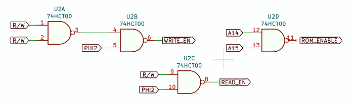
An open gate
I mentioned the 74HCT00 has four NAND gates and we've so far used three. What could we do with the other one? The answer is: decode the ROM.
If you look at the address map above you'll see that the ROM addresses start at $C000. Another way of putting that is: $8000 + $4000. And you get those values by setting pins A14 and A15 of the address bus high.
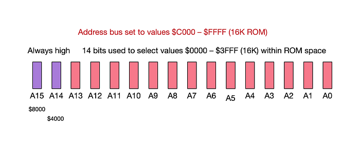
If we connect both A14 and A15 to the inputs of the NAND gate, the output will be low only when both of the inputs are high — ie, when the CPU wants to talk to the ROM. Only the addresses in the ROM space will have both those pins high — every other address sets at least one of those pins low.
So, we connect the output of this fourth NAND gate (which I've labelled /ROM_ENABLE) to the /CE of the ROM chip and now we have the ROM decoded.
But what about qualifying the signal? I haven't mentioned anything about the clock signal. Well, we've already created a clock-qualified /READ_EN signal, so we just connect this to the ROM's /OE pin and now everything is suitably gated. (We only read from the ROM, we don't write.)
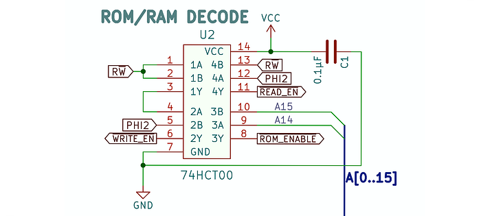
Here's how it looks on the schematic.
This is all very basic decoding. For the I/O sections of the memory map, we're going to have to resort to something a little more sophisticated. That's coming soon.
You can find all the stories related to this project on the Zolatron feature page.
There is also a GitHub Zolatron repo with the code, datasheets and other documents.
Steve Mansfield-Devine is a freelance writer, tech journalist and photographer. You can find photography portfolio at Zolachrome, buy his books and e-books, or follow him on Bluesky or Mastodon.
You can also buy Steve a coffee. He'd like that.
My Friend retro games NES SEGA