ELECTRONICS
Breadboard and protoboard are all very well, but pretty they ain't. With breadboards, wires and components work their way out of the holes at the slightest provocation, and your beautifully conceived and elegantly designed project always ends up looking like the mice have had a party.
Protoboard or stripboard is better, in that the pieces are generally soldered into place. But it's never the optimal solution.
Now that it's relatively cheap to have PCBs made, I habitually celebrate the completion of a project by having a board fabbed — once I'm absolutely convinced everything (bar software tweaks) is working as it should.
To fab or not to fab
I said 'relatively cheap' because it's still not low cost by any means. And that means moving the project to the final stage of a custom PCB is not automatic. For some people (like me) who must count their pennies, it's a decision that needs to be carefully considered — not least because you might make a mistake and find that (at best) you have to sully its beauty with bodge wires or (at worst) your PCB now functions best as a coaster.
A case in point: with my infrared IoT hub project, I ended up with working prototypes for most of what I wanted to achieve. And what wasn't working was due to software. I created schematics and designed PCBs for the two devices partly as a way of documenting them and also just for fun. But I held off having them fabbed.
Until, that is, PCBWay reached out to me and offered to supply free boards as a way of supporting Machina Speculatrix. As a retired person on a very limited income, this was too good a deal to pass up, but I did have some strict conditions (to which PCBWay readily agreed). The main one is that, as someone who earned his living from journalism, I'm very insistent on editorial independence, so PCBWay would have no control over what I write. For more info, see the section on sponsorships and support at the end of About Machina Speculatrix.
Basic boards
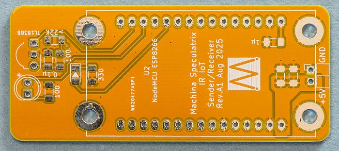
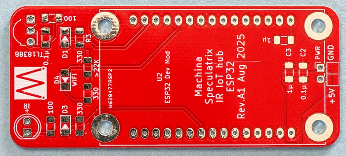
To be honest, I wasn't going to tax PCBWay's capabilities very much. These are extremely basic PCBs, mostly just female headers to plug in the ESP boards plus the IR sensor, an IR LED and a bunch of supporting passives.. That said, I decided to go with a four-layer stack-up. It would have been trivial to create these devices with two-layer boards, but the extra cost of four-layer is small these days and I like having nearly uninterrupted internal power and ground planes. (The main fills on the top and bottom layers were also connected to ground.)
I'll show the schematics for both boards although, given their simplicity, I'm not sure why.
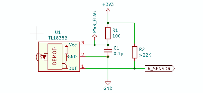
Here's the part of the schematic that's common to both boards, which is the wiring up of the IR receiver sensor. I covered this in detail in the previous article.
Power supply
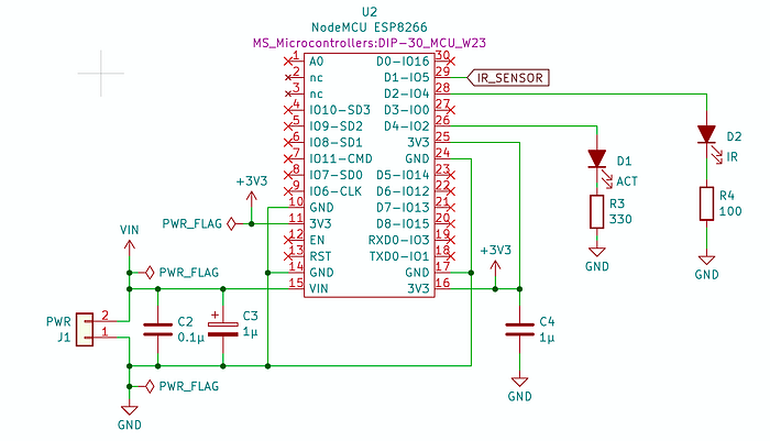
Something else both boards have in common is that I'm using the +3.3V regulated output from the ESP microcontrollers to drive the sensor. That ensures the data signal from it is 3.3V, which is what the ESPs expect on their GPIO pins.
The microcontroller itself gets +5V power either from the USB cable plugged directly into it or via +5V you supply to the power pins. The various LEDs are driven by the microcontroller's GPIO pins, so the only thing that needs power, other than the MCU, is the IR sensor.
For most of the components — LEDs, resistors and capacitors — I went with surface-mount variants. This keeps the board size small and also let me put some of them underneath the microcontrollers.
I tend to stick with the 1206 size for SMD passives because anything much smaller is a challenge for my shaky hands.
For the power supply, I chose simple header pins. In hindsight, perhaps a USB-C connector would have been a better bet, but I was aiming for simplicity. There is no polarity protection: wire the +5V and GND the wrong away around and unpredictable behaviour will ensue, although it's likely to involve smoke. However, I did remember to clearly label which pin is which on the silkscreen. That's not something I've always managed to do.
Now let's look at the two PCB designs.
ESP8266 sender and receiver
This is intended to be one board to create two separate devices.
This board has both an IR LED for sending signals and a sensor for receiving them. The idea is that you solder one or the other to the board depending on whether you want:
- A device that receives MQTT messages and emits corresponding IR signals; or
- A device that senses IR signals, decodes them and transmits suitable MQTT messages over the network.
Or … you could solder all the components on the board and decide later which function it will fulfil based on which version of the software you upload.
Besides the sensor and IR LED, there's one other LED (D1) which I've marked ACT to indicate activity. You can use this for any purpose your heart desires. I like putting these LEDs on boards because there's a surprising amount of software debugging you can do simply by flashing an LED.
ESP32-based IR hub
This is the device that's intended to be used as both a sender and a receiver. I also plan to use it as the basis for learning about FreeRTOS and multitasking on ESP32s — something I clearly know far too little about.
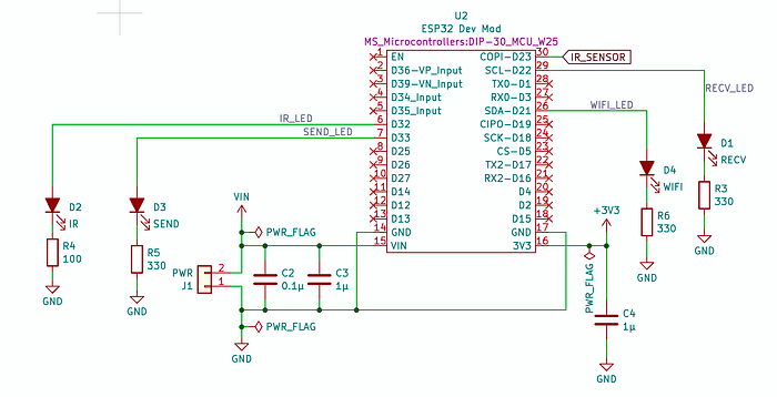
This board has more activity LEDS than the 8266 one. In the current code, the WIFI LED flashes to show when the board is acquiring a wifi connection; the SEND light flashes when an IR signal has been sent; and the RECV light similarly flashes when an IR signal has been received. Again, you could always amend the code to get these LEDs to signal whatever states or activities you find most interesting.
Board layout
Laying out the PCBs was trivial due to their simplicity. But there were a few decisions I made.
First, the boards have rounded corners because … pretty.
Second, I added four mounting holes for M3 screws. This to help in case I decide to house the devices in project boxes. In the meantime, I can use the holes for standoffs so that the underside of the PCB isn't resting on anything inconvenient, like a conducting surface. I like using brass standoffs because the weight aids stability. All the mounting holes are through-plated and connected to the ground planes.
There were no difficult routing decisions to make — how could there be? However, one choice I did make concerned the Vin supply to the microcontroller.
I could have run traces from the +5V pin on the header to the relevant pin on the MCU, via the two decoupling capacitors. Instead I opted for a +5V copper pour. In the image below, the main (reddish coloured) area is a GND pour. But the shape on the left-hand side is +5V.

Ordering the boards
PCBWay's online ordering form can seem daunting to the beginner because there are so many options, but here's a tip. As a beginner you'll mostly want to stick to the defaults. If in doubt about any setting, leave it alone.
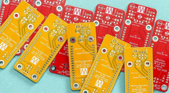
I went with different colour solder masks so that I can tell which board is which without reading the silkscreened text (my eyes aren't what they used to be). The colours I chose — yellow and red — added no cost above the standard green, which isn't necessarily the case at all fab houses. Blue, white and black were also available for the same price, but you will pay more for purple, matte green or matte black.
As with other fab houses I've used, the big cost isn't the manufacture of the boards but the shipping (I'm in France). However, PCBWay does have more options than most, including ones that will handle import fees and taxes for you — so no nasty surprise when the delivery person shows up with a bill. I recommend spending some time working out the best option for you and your location.
The boards shipped four days after ordering and were in my eager little mitts three days after that.
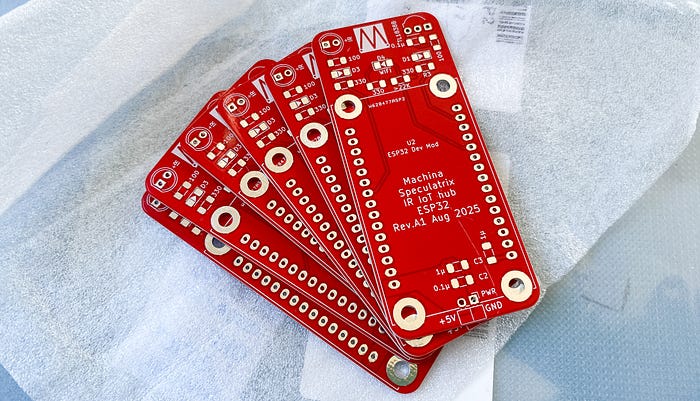
They came well-packaged, wrapped in that fleece-like paper and sealed, with a bag of silica gel, inside plastic bags.
Companies like PCBWay can afford to offer us humble hobbyists cheap PCB fabbing because they use our orders to fill otherwise unused space on large production panels. One upshot of this is that you can, on occasion, get more than you paid for. I ordered five of each board (the minimum) but received six of the ESP32-based model. This has happened to me several times in the past. It's not something you can count on but is a nice bonus when it happens.
The PCBs are every bit as professionally produced as you'd expect. Like I said, they didn't really present much of a challenge, but I am nonethless very happy with the crispness and accuracy of the silkscreening and solder masks, as well as the quality of the solder pads.
Making up the boards
Both boards contain a mix of surface-mount and through-hole components. My preferred soldering method for surface mount is to use a toaster oven controlled by a custom timer device to carry out reflow soldering. (If you'd be interested in an article on my journey of discovery with surface mount soldering, let me know in the comments.)
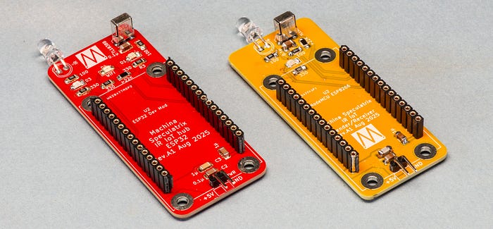
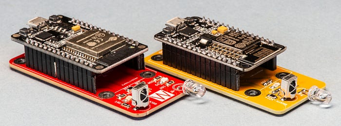
As it happened, I'd not stored the solder paste well and had only enough for one of the ESP32 (red) boards. The rest of the paste was solid. I hand-soldered the ESP8266 (yellow) board, which was quite the challenge (remember how I mentioned my shaky hands?).
The good news is that both boards work fine and look great (in my opinion), so long as you don't stare too closely at the soldering.
And as always, having working PCBs has brought a sense of completion to the project. Except that I still have a lot of coding to do as I try to push the capabilities of the boards. But that's for another day.
All the code for this project, plus Gerbers and schematics for the PCBs, is available on GitHub. Thank you to PCBWay for supporting this project by supplying free PCBs.
Steve Mansfield-Devine is a freelance writer, tech journalist and photographer. You can find photography portfolio at Zolachrome, buy his books and e-books, or follow him on Bluesky or Mastodon.
You can also buy Steve a coffee. He'd like that.
My Friend retro games NES SEGA