
PROGRAMMING
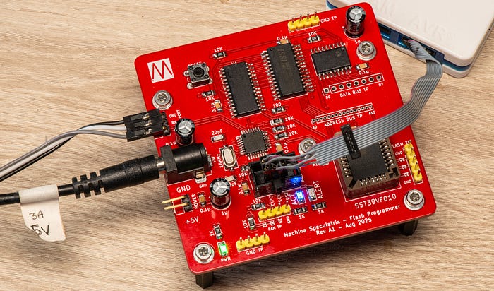
Just a quick recap, the flash ROM development board I designed allows you to store binary code in a flash chip so that you can use the chip in place of a ROM (or EEPROM) in a homebrew microcomputer.
The dev board is intended to allow me to create and play with software. Ultimately, the aim would be to integrate its main functions into a module within the homebrew machine itself.
Purpose of the software
Pushing the ROM image to the dev board and writing to the flash involves two pieces of software — firmware for the dev board's own microcontroller and a 'terminal' program (at least, that's what I'm calling it) that runs on a PC and controls the whole operation.
Both of these pieces of software exist. And they work in the sense that all the functions are in place to upload a ROM image from a PC to the dev board and store it in RAM, and to write that code from the RAM to the flash chip. But I hit a few bugs. Are you surprised? I'm not.
At least, that's the state of affairs as I write this article. The software is under sporadic but fairly frequent development right now, so for the latest version, you can check the GitHub repository for this project. I may also provide minor updates via the Lab Notes newsletter.
I'm not going to provide a line-by-line breakdown of the code. For one thing, I don't imagine anyone else will use it and it contains no ground-breaking work. What I think we should focus on here is the overall design concept. So let's get into it.
Microcontroller firmware
The firmware on the ATmega328PB spends most of its life in the main loop waiting for a message to arrive via the serial port. There are four principle messages it understands:
DNLDfor 'download' (not 'Donald'. Definitely not that). The MCU accepts a stream of binary data from the PC over serial and writes it to RAM.FLSHfor flash. The MCU copies the data in RAM to the flash chip.READ. The MCU reads a block of data from the flash chip, starting at an address supplied, and sends it to the PC.SRAM. Similar to READ, but this pulls a block of data from the SRAM to send to the PC.
A lot of the operations are built around a couple of functions. For example, the following function takes a 16-bit address and eight-bit data value and places those values on the relevant buses.
void flashWrite(uint16_t address, uint8_t value) {
    addrport.setWord(address);
    dataport.setByte(value);
    setPin(&PORTC, FL_WE, LOW);     // latches address
    _delay_us(FLASH_BYTE_DELAY);    // pause for effect
    setPin(&PORTC, FL_WE, HIGH);
}
The addrport and dataport objects use my own classes for controlling the MCP23017 and MCP23008 port expanders. (These classes are in the GitHub repo, as are my underlying I2C device class and my class for serial communications.) The details aren't important—the key here is that the buses are set to the appropriate values, the MCU pin attached to the flash chip's write enable (/WE) pin is taken low, there's a brief pause, and then the pin is taken high again.
This function is at the core of all write operations — including writing a byte and erasing a sector. As an example, here's the code for writing a byte:
void flashByteWrite(uint16_t address, uint8_t value) {
    setPin(&PORTC, FL_CE, LOW);     // enable flash chip
    flashWrite(0x5555, 0xAA);
    flashWrite(0x2AAA, 0x55);
    flashWrite(0x5555, 0xA0);
    flashWrite(address, value);
    setPin(&PORTC, FL_CE, HIGH);    // disable flash chip
}
You can see how it uses a sequence of write operations. The function makes the flash active by taking its chip enable (/CE) pin low, then sends a sequence of three special values (0xAA, 0x55 and 0xA0) to special addresses (0x5555 and 0x2AAA). This is a command sequence telling the flash chip that the next values on the address and data buses will be a byte value to write to that address. I went over this in more detail in a previous article.
Reading from the flash chip is a lot like reading from RAM.
uint8_t readFlash(uint32_t address) {
    uint8_t value = 0;
    addrport.setWord(address);      // set address bus
    setPin(&PORTC, FL_CE, LOW);     // enable flash chip
    setPin(&PORTC, FL_OE, LOW);
    _delay_us(FLASH_BYTE_DELAY);
    value = dataport.readByte();
    setPin(&PORTC, FL_OE, HIGH);
    setPin(&PORTC, FL_CE, HIGH);    // disable flash chip
    return value;
}
We set a value on the address bus for the byte we want, take the flash chip's /CE and output enable (/OE) lines low, wait a brief moment, read the value on the data bus and then take /CE and /OE high again.
It's all fairly straightforward, although if you have any questions about the code, feel free to ask by leaving a comment.
PC Python
The code running on my dev PC (an old MacBook Air running MX Linux) is essentially just a serial terminal customised to our specific needs. It's written in Python and, because I have a fondness for old-style terminal programs, I also used Curses.
The PC connects to the dev board via a USB-to-serial (FTDI) cable. There's no hardware flow control, so only three connections are required — TX, RX and GND. On my machine, the adapter appears as the device /dev/ttyUSB0, and this is what I have hardcoded into the program. In future versions I'll allow for this to be set with a command line flag and possibly via the menus.
Similarly, the serial speed is 9600 baud because I generally find that a safe starting point for any project involving serial. I will probably build in the option to change that, although my one-and-only attempt so far to use 19,200 didn't go so well. That needs looking into.
The code is menu-driven, in the time-honoured fashion. The options are:
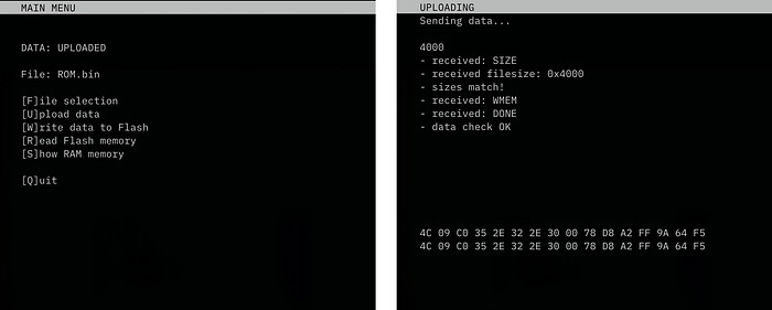
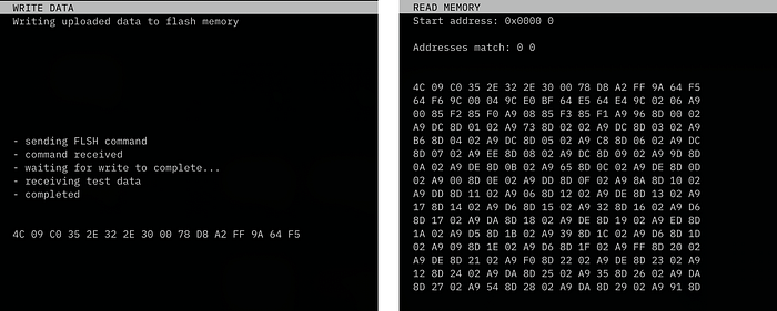
[F]ile selection: this allows you to choose the name of the file containing the binary ROM image. The file needs to exist in afiles/subdirectory of the current working directory. The filename defaults toROM.bin.[U]pload datadoes what it says — it transfers the binary data from the file to the dev board's RAM. The first 16 bytes of data are returned so that the Python code can check them against the first 16 bytes of the image file, as a simple error check. The two sets of data are presented on the screen for confirmation.[W]rite data to Flashtells the dev board to go ahead and write the data in its RAM to the flash chip.[R]ead Flash memory: this prompts for a four-digit hex address and reads the 256 values in flash memory starting at that address. It's a way of checking that that things have gone as planned.[S]how RAM: this also prompts for a four-digit hex address and then reads and displays the 256 values in SRAM memory starting at that address. It's for checking that the upload proceeded smoothly.
Good communication
The communications between the board and the PC have some error checking built in. For example, when the board receives a command from the PC, it usually echoes it back so that we can spot any communication breakdown.
Similarly, there's some checking that, say, the address value sent is the same as the one received.
But it's not foolproof. The code could do with a little more error checking and also exception handling on the part of the Python code.
I have a tendency to accept crashes as nature's way of telling me what's wrong with my code. And that's because I write code for myself — it doesn't have to be 'production ready'. If it runs most of the time without locking up or blowing up, that's a win. As a hobby programmer, you can waste of lot of time on non-critical stuff. My rule is to keep improving the software until a shiny new project grabs my attention.
Remaining issues
Like I said, all this works(-ish). So what's the problem? It's largely a matter of bounds checking and sanitising. Currently, when you ask to read data from flash or SRAM there's no check to ensure that the address you provide is viable. The file selection routine is probably prone to all manner of user input-related crashes. In other words, it's all rather rough.
Some of the bugs were interesting. I had a problem where the data was uploading to the SRAM fine, but when I came to write it to the flash, the first three bytes of each sector always ended up being 0xFF. This seemed suspicious. That's the value written to each byte during the sector erase process. Was the program trying to write data bytes before the chip had finished erasing the sector?
My code for erasing a sector looked like this:
void sectorErase(uint16_t startAddress) {
    setPin(&PORTC, FL_CE, LOW);     // enable flash chip
    flashWrite(0x5555, 0xAA);
    flashWrite(0x2AAA, 0x55);
    flashWrite(0x5555, 0x80);
    flashWrite(0x5555, 0xAA);
    flashWrite(0x2AAA, 0x55);
    flashWrite(startAddress, 0x30);
    _delay_us(FLASH_SECTOR_ERASE_DELAY);    // allow the dust to settle
    setPin(&PORTC, FL_CE, HIGH);            // disable flash chip
}
Don't worry about the details. The key bit is the delay after all the write operations. The datasheet says you have to give the chip a moment to finish, and so I'd set FLASH_SECTOR_ERASE_DELAY to the recommended value of 25.
Thinking that maybe it needed just a little more time, I increased the value to 30, then 50, the 100, then 255 — all to no avail. Then I tried adding another delay of an entire second. That worked! But it was obviously not a sensible value. So I headed back to the datasheet.
And it still said 25. But then I noticed something. It was 25ms, not 25µs. I changed _delay_us(FLASH_SECTOR_ERASE_DELAY); to _delay_ms(FLASH_SECTOR_ERASE_DELAY); and now all is working fine.
The moral of that story? Once you've read the datasheet, read it again.
So, there is work to do, but the bones of the thing are in place and I feel that the proof of concept is proven. My intention with this code, and this article, was to wrap up the project. But it is going to continue is a way.
Because I got to thinking (always a dangerous thing). Given that this project was inspired by my desire to write ROM images directly to the Zolatron, is this actually the best way to do it? In a forthcoming article, I'll be exploring both the problems with this approach, ways of modifying it, and an exciting alternative.
There's a GitHub repo for this flash programmer project, which includes schematics and Gerbers for the PCB, C++ code for the ATMEGA328PB and Python code for the PC.
The articles relevant to this project are:
- Using flash memory as a homebrew computer ROM.
- A development board for flash-based ROM.
- Software for the flash ROM development board (this article).
Steve Mansfield-Devine is a freelance writer, tech journalist and photographer. You can find photography portfolio at Zolachrome, buy his books and e-books, or follow him on Bluesky or Mastodon.
Sign up for the Machina Speculatrix Lab Notes newsletter.
You can also buy Steve a coffee.