MICROCONTROLLERS
Let's be honest, we all enjoy indulging outselves in a bit of fun with chips. However, if you find yourself having fun with a particular chip on more than one occasion, you end up repeatedly recreating the same basic circuit on a breadboard, which is a tad tedious.
Another issue is that not all chips come in breadboard-friendly formats. I realised this when I started messing with PLCC and QFP packages.
On those occasions where I think I'm going to develop multiple projects or run a variety of experiments around the same chip — or need easy access to the pins — I like to build myself a breakout board. It saves a lot of time.
AVR microcontrollers
This all started with the Arduino Uno. That was my introduction to microcontrollers (MCUs) and I bought a lot of the little blighters. Then I realised there isn't much to an Arduino and I became interested in using the core microcontroller, the Atmel ATMEGA328P, in its native state. That way I could start building the MCU into my projects, rather than bolting on a whole Arduino dev board. That also led me to programming the chip outside of the Arduino environment. But how would I go about flashing the firmware?
My programming device of choice is the Atmel-ICE, an in-system programmer (ISP). This has a cable with a six-pin ISP header that you need to connect to the CIPO, COPI, SCK and RESET pins of the chip as well as the VCC and GND of your circuit. With those connections made, you can perform in-circuit programming.
And so I bodged together a 2x3 IDE socket with a bit of stripboard to create an ISP header that I could plug into a breadboard. But that still left me with the chore of setting up the rest of the MCU basics, including the chip itself, a crystal, some capacitors, power supply and the connections between the ISP header and the chip.
Moving up
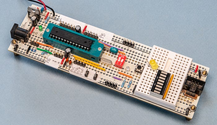
The next step was to move up to protoboard and I chose one that is designed to mimic breadboard, with rows of connected pins and power rails.
The microcontroller went in a zero insertion force (ZIF) socket. I soldered in a 16MHz crystal and supporting 22pF capacitors, a barrel jack socket for power and a linear regulator for a solid 5V, plus a power LED and the ISP header.
Then I got creative. I connected an LED and a tactile switch to pins PB1 and PB2, but via DIP switches so that I could use the pins for other purposes if I wanted. As a final flourish, I glued on a mini-breadboard.
And what did I have?
An Arduino Uno, essentially. So why not use an Arduino Uno?
Fair point. Except that my rig does have a couple of advantages. For a start, once the chip is programmed, I can easily remove it to plonk it into a project. And there's that handy LED and the pushbutton. Besides which, this was just a stepping stone.
Improving matters
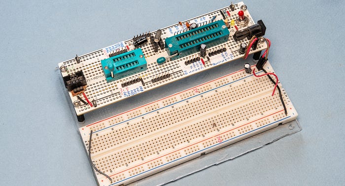
Version 2 improved on the design by adding a power switch, a removable crystal simply mounted in female headers (in case I wanted to try other speeds or use the internal crystal) and a reset button, although it did away with the optional LED and pushbutton (I can't remember why).
But the biggest improvement was the addition of a second ZIF socket to accommodate ATTINY84A chips.
I mounted the protoboard alongside a breadboard on an acrylic base. It works great and remains my go-to prototyping rig for the ATTINYs. But not necessarily the ATMEGA328P.
Go small or go home
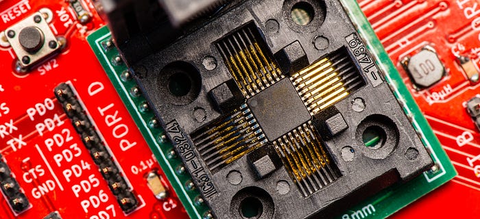
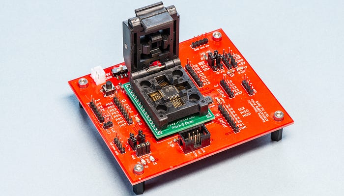
Once you've discovered the space-saving joys of surface mount devices (SMDs), there's no going back. The SMD version of the venerable 328 is the ATMEGA328PB which comes in the tiny but not prototyping friendly TQFP format (at least, mine do. VQFN versions are also available).
The 328PB has a slightly different configuration of ports to its DIP sibling and so I couldn't simply plug an adapter board into my current prototyping rig. Instead, I went for a whole new board — and, this time (and forever going forward) on a PCB instead of protoboard.
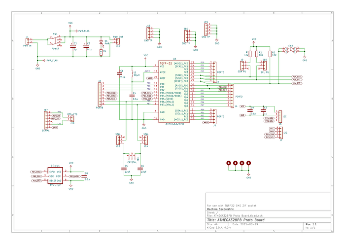
I built this around a TQFP ZIF socket. This cost $16 from one of the well-known Chinese suppliers, which isn't exactly cheap.
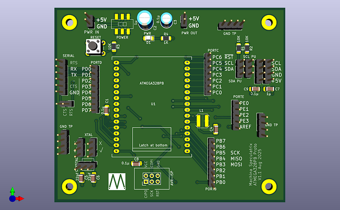
Besides breaking out all the GPIOs to header pins and the essential power supply and switch, reset button and ISP socket, the board doesn't boast any partiularly clever features. I added optional pullups on the main SDA and SCL lines for I2C (you select them, or not, using jumpers).
I also added female headers for a removeable crystal, but with jumpers so that you can disconnect the crystal and its capacitors entirely to use the internal clock.
The board has an inductor between AVCC and VCC, plus a capacitor to ground, forming a low-pass filter. Why? Because the datasheet says so and I'm not going to argue.
I use this board occasionally for experimenting but not so much for programming chips before soldering them into projects (which is what I thought I would do). Instead, I tend to add an ISP header to each project so that the chip can be programmed in situ.
When I came to review the Kicad files for this board, in preparation for this article, things got a little messed up. This was due to having moved on several versions of Kicad (I created the original files in 2019) and because I've since changed certain custom symbols and footprints. So the current version is now 1.1, which I haven't had fabbed yet. But here's Kicad's rendering of it.
Das blinkenlights
That didn't entirely slake my thirst for ATMEGA prototyping boards, though.
On the very first board, I included that optional LED because there's an awful lot of software debugging you can do just by making a light blink. It tells you what a GPIO pin is up to. But what if you want to know what all of them are doing?
I found myself wanting to monitor the state of a bus — sometimes eight lines, sometimes 16. Wiring that many LEDs into a breadboard is not fun. It's made easier with bar LEDs and resistor packs, but still…
The next board took me back to the DIP version of the ATMEGA328P. This time, the chip is in an ordinary socket, not a ZIF, because this is very much about experimenting and not for programming chips for use in other devices.
The 16MHz crystal is soldered in but connected via DIP switches so that I can disable it. And the only other feature of note (bar one that we'll get to) is the presence of two pushbuttons. These don't connect directly to GPIO pins but to standard header pins for use with jumper wires. But both buttons are hardware debounced.
The main attractions, though, are the rows of LEDs, one for each of the three GPIO ports with an LED for every pin. That's 22 LEDs in all. It's mesmerising watching the state of the pins as a program runs.
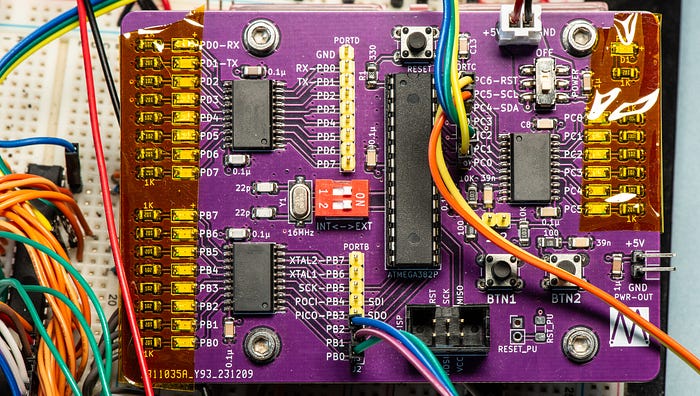
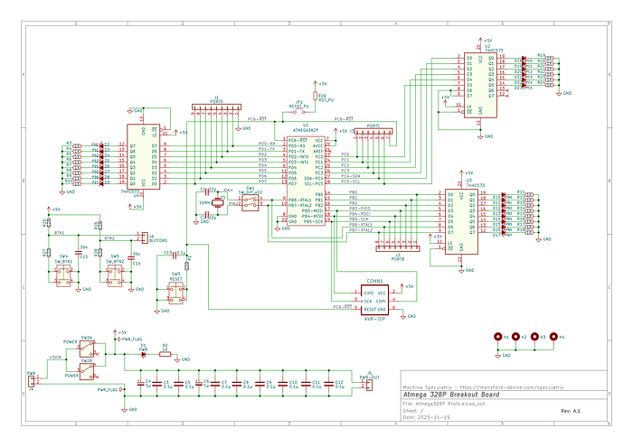
I didn't want to have to drive the LEDs directly from the GPIOs as that could cause all manner of issues. Instead, the LEDs are connecting to the GPIOs and driven via 74HC573 octal transparent latches. And driven they certainly are. Even with 1KΩ power-limiting resistors, they are rather on the bright side.
And yes, it's basically an Arduino Uno again, but with all those lovely blinkenlights.
Complex logic
The Complex Programmable Logic Device (CPLD) is a fine thing. With a little bit of programming (although purists don't like to call it that) you can create your own IC incorporating all manner of logic operations. I know because I've done it.
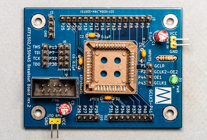
The CPLDs I chose to play with are the ATF150xASL family — specifically the ATF1502ASL and ATF1504ASL. These come as PLCC packages, which didn't present much of a problem because I also invested in the Atmel ATF15xx-DK3 development/programmer kit. This is the very definition of not cheap, but it does offer a rich variety of onboard switches, buttons, LEDs, seven-segment displays and more. It also works with multiple versions of the chip (eg, TQFP as well as PLCC).
For experimenting with and learning about CPLDs it's great and I'm glad I could apparently afford it back then. However, once I'd got my teeth into CPLDs, I actually needed something considerably simpler for integrating into project prototypes. In other words, a breakout board.
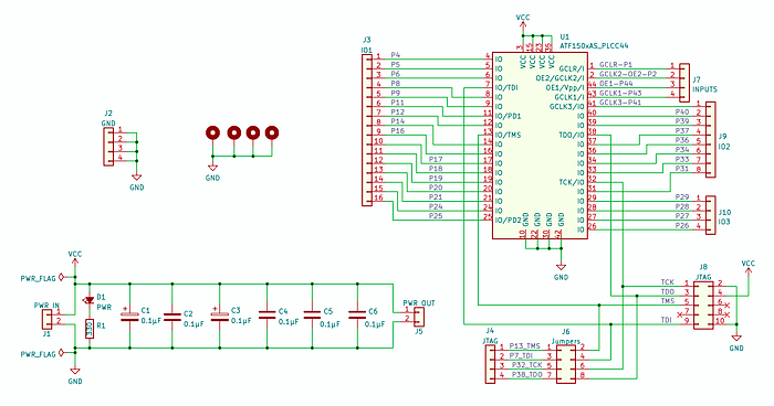
And that's all this is. It has the pins broken out to headers, a JTAG header for the programmer, some decoupling caps, a power input with LED and power out pins to daisy chain with, say, a breadboard.
The only refinement consists of four jumpers. Pins P7, P13, P32 and P38 are used for the TDI, TMS, TCK and TDO signals. But you need them for those functions only when programming the chip via the JTAG header.
With no jumpers in place, the four signals run only to the JTAG header. With a jumper in place, each signal also runs to a header pin.
Flash memory
Flash memory is a great replacement for ROMs and EEPROMs. And the flash memory chip I'm most interested in is the Microchip SST39SF010 with 1Mbit of memory, but this board also works for the 020 (2Mbit) and 040 (4Mbit) variants.
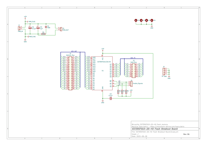
It's just a breakout board. The only thing I've added are three resistors to pull up the /WE, /OE and /CE lines, which are all active low.
I wanted a way to experiment with flash chips — and especially the PLCC package variants. So this board naturally has a PLCC socket.
I originally played around with the 3.3V versions of the flash chip (the SST39VF010), and the silkscreen on the board in the photograph reflects this. (Although it also mistakenly labels the power input as +5V. Oops.) Pretty soon I switched to the 5V devices and so kept the +5V label. In hindsight, I probably should have just used VCC. The board doesn't care which version of the chip you use, nor which voltage. Just attach +5V for the 'SF' versions of the chips and +3.3V for the 'VF' versions. Of course, if you get the voltage and chip combination wrong … well, you're going to have an entertaining day.
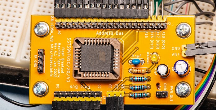
There's a couple of capacitors to keep the input power steady, power out pins and a power LED to show the board is alive. And that's all there is to it, except…
Adding holes
Mounting holes are essential for prototyping boards like this. You want the thing to be stable, so at the very least I'll mount them on brass stand-offs to give them weight.
Just as often, I'll mount the boards to a thick acrylic sheet, often alongside other prototyping boards or breadboards.
I use through-hole plating for the mounting holes and connect them to ground. That makes them useful as ground test points.
I've pretty much standardised on M3 as my favourite size for stand-offs and screws, so that's the size I've used for the mounting holes.
Test points
Another habit I have — and not just for prototyping boards but PCBs in general — is that of adding test points. I generally find that when things don't work as expected, it's good to know why. Test points help enormously with that.
I'll add points for what I consider key signals. What qualifies for that category is a judgment call. But put yourself in the position of the future you struggling to get either the board or your software working. Which signals are most likely to inspire the thought, 'I wish I knew what that thing's doing'?
My test points are typically standard pinheaders (2.54mm pitch). Sometimes I'll populate the TPs with actual headers. Other times I'll just stick my oscilloscope or multimeter probes into the holes.
I also add a small row of pinheaders all attached to ground. These become a handy place to attach the ground leads of oscilloscope probes.
You do you
While I'm showing the schematics and have made the Gerber files available, I'm not suggesting you build these actual boards or copy my (possibly sub-optimal) ideas.
I just wanted to share my approach in the hope that you would find it useful, and maybe even inspirational. Building your own tools is a great way to explore and understand a technology, such as a microcontroller.
You can find the schematics and Gerber files for most of these boards in my GitHub repository. These are offered as-is, with no guarantees, warrantees or any other 'tees. Use at your own risk and for your own entertainment.
Steve Mansfield-Devine is a freelance writer, tech journalist and photographer. You can find photography portfolio at Zolachrome, buy his books and e-books, or follow him on Bluesky or Mastodon.
You can also buy Steve a coffee. He'd like that.