Having settled on the idea of using flash memory to hold ROM images for my 6502-based homebrew computer — and also having worked out how to program flash chips — the next stage was to develop code.
Not just one program, but two. But that would still have to wait for a while because first I needed better prototyping kit.
Basic concept
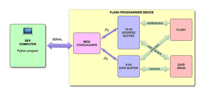
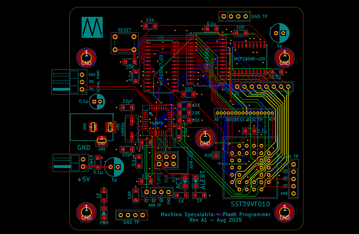
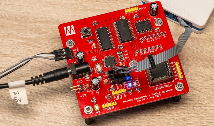
The basic concept revolves around a programmer board that has the flash memory, some SRAM and a microcontroller that handles the downloading of the data to burn to the chip and the flashing itself. This MCU talks via serial to a PC that is running a Python program to control the functions of the MCU and upload the ROM images.
And to learn how to do all this I had to design a programmer board that would allow me to play with software and (foreshadowing) maybe decide if this was the best way of going about things.
This article covers what I came up with in terms of the board. The code — and some alternative ideas — will be in future articles.
But first, please note that this is a proof of concept design to allow me to develop code and understand the whole process. I'm sure it can be optimised in many ways. For example, it could definitely benefit from a much faster microcontroller. Also, the software is in an eternal alpha state, and I will be twiddling with it constantly. If you look at the GitHub today, consider what you find there as just a hint of glories to come.
This isn't meant to be an all-purpose flash programmer. But if you have the need to program flash chips, I hope it will give you ideas you can implement for your own projects.
Breadboard prototype
For the breadboard prototype, I'm using an AS7C256B 32KB SRAM chip, which has a 15ns access time, because it's what I had to hand in DIP format. For the PCB, this will be replaced with a SOP-format IS65C256AL, which is actually slightly slower (25ns) but that's still plenty fast enough for me and it's around 3€ a pop on Mouser.
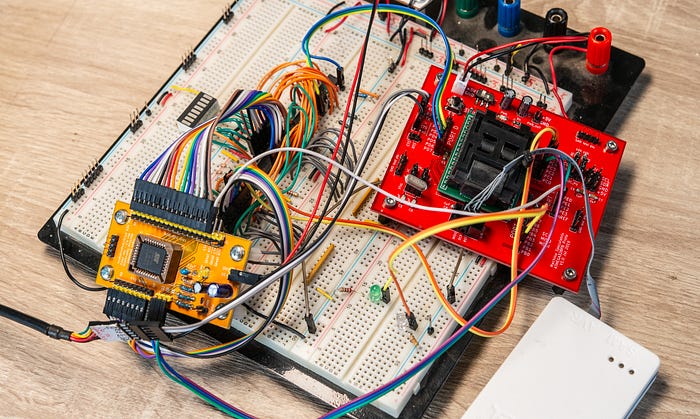
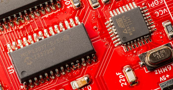
The ATMEGA328PB — one of my go-to microcontrollers — is well supplied with GPIOs. But this board needs a lot. The answer was to offload the task to intermediate buffers, in the form of port expander ICs. An MCP23008 gives us eight I/O pins for the data bus and an MCP23017 provides 16 I/O connections for the address bus. Both chips have I2C interfaces, so between them they require just two pins on the MCU.
The port expander for the address bus only ever needs to output values, not read them, so setting the data direction for that is simple.
The data bus port expander must be switched between input and output modes, depending on whether the MCU wants to read or write data. But that's easy enough with these chips, and we're setting the mode for the whole device at once, because at any given time we're either reading or writing on a bus, not a mix of the two. So that's easy enough.
Not enough lines
There's one slight shortcoming with this arrangement — that there are only 16 address lines. This allows us to address a maximum of 64KB, but the capacity of the SST39SF010 flash chip we're using is 128KB (1Mbit), for which it has address pins in the range A0-A16.
At first glance, this doesn't seem like an issue. The ROM images we're working with are only 16KB anyway. We could just use the bottom 16KB of the flash memory and be satisfied.
And yet that unused capacity nagged at me. It would be so nice to be able to write multiple ROM images to the chip and select between them in some way. And for that we need control over all of the address lines.
I started by having the flash address pin A16 permanently tied low, which would have been fine for my current experiments. Later, I used a spare GPIO on the MCU to control this pin. But at the moment, I'm just setting this pin low in software. I can always refine the code later.
If we want to make use of the 2Mbit and 4Mbit versions of the chip, we would need to think about handling extra address signals. Replacing the 8-bit MCP23008 used for the data bus with a 16-bit MCP23017 might be one option, although it will make the coding somewhat more complicated. Alternatively, we could exploit currently unused GPIOs on the microcontroller. Something to think about, but not now.
More detail
Let's go through the circuit design in a little more detail.
The following schematic is the design as of early September 2025. Things are likely to change. You can always find the current version in the GitHub repo.
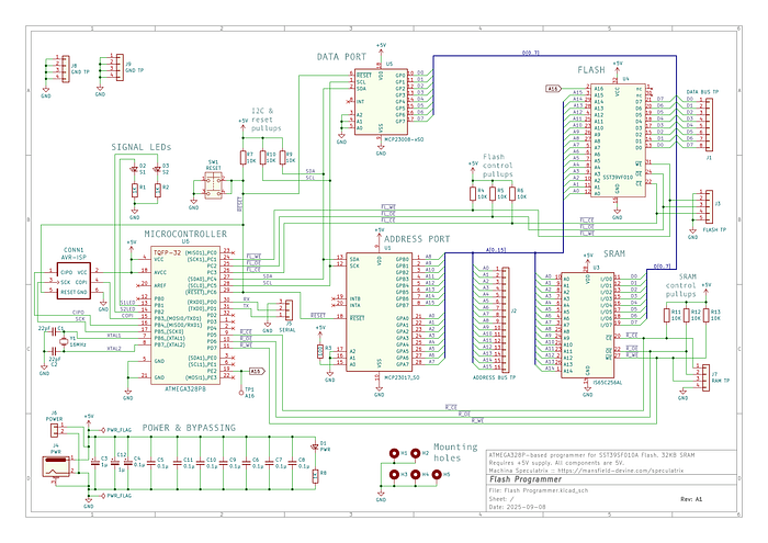
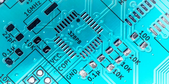
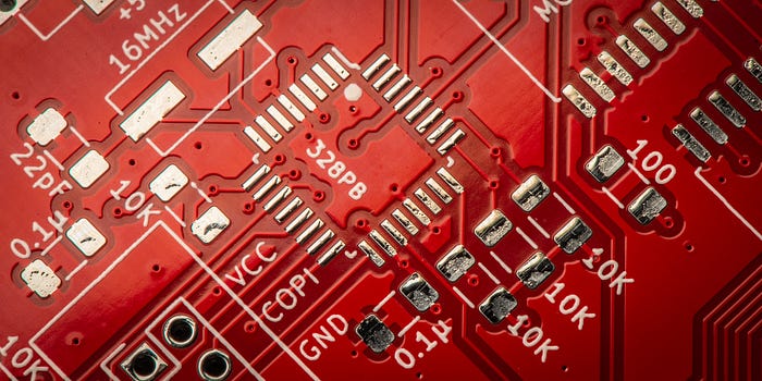
The ATMEGA328PB microcontroller is being clocked at 16MHz with an external crystal. Three GPIOs control the chip enable (/CE), write enable (/WE) and output enable (/OE) signals for the flash chip. Another three control the same signals for the SRAM. All six of these lines have 10KΩ pullup resistors.
The I2C pins (SDA and SCL) of the MCU connect to both the MCP23008 and MCP23017 port expanders. And again, both lines have pullup resistors.
There's a pushbutton (tactile switch) that grounds out the reset pins of the MCU and both port expanders, all of which are on a common line which — you guessed it — has a pullup resistor. I find reset buttons to be remarkably useful when developing hardware and code.
Each port expander needs a unique three-bit address by setting the values on pins A0, A1 and A2. For the MCP23008 (driving the data bus) I've tied all the pins to ground, giving an address of 0. On the MCP23017 (the address controller), pin A0 is tied high (via a resistor) while the other two are connected to ground, giving an address of 1.
Actually, because of how things work in the I2C world, these create addresses 0x20 and 0x21, respectively.
And because there are MCU GPIO pins going spare, I've wired up a couple of LEDs that I'll use for showing activity and for help with debugging.
Throw in a power LED, decoupling capacitors and a bunch of test points and there you have it.
PCB design
Moving up to a PCB design presented no major headaches. I'll go into some detail — not as advice but as an invitation for constructive criticism.
I went with a four-layer board because it's just so much easier. Most of the parts are surface-mount, for compactness. And while I normally use 2.54mm pitch headers for test points, for the 16 address lines I went with a much finer 1.27mm pitch. (To be completely honest, I accidentally selected the 1.27mm pitch and chose not to correct it.)
Maybe I should have gone for the larger pitch, but it would have taken up a lot of board real estate. And I probably won't actually solder in headers anyway. The footprint is enough to allow me to prod the board with an oscilloscope probe.
The are two options for power input — a 5.5x2.1mm barrel jack connector and plain old pinheaders. As usual, I provided no polarity protection because I like to live dangerously.
I decided to be generous with the mounting holes. As well as one in (roughly) each corner, I put one in the middle, near the AVR-ISP and flash sockets. You're going to be pushing a connector or chip into these sockets regularly, so having a standoff nearby will help prevent board flexing.
Routing threw up a few challenges. I always route manually, because that's how you learn. And besides, it's fun, in a puzzle-solving kind of way. In the end I had to route some tracks on the inner copper layers, which I generally like to keep as pristine as possible (bar vias) for the ground and power planes. In the picture above, red traces are on the top layer, yellow ones on the second (+5V) layer, blue on the third (GND) layer and green on the bottom layer. There are ground pours on the top and bottom layers, too.
What's in a name?
There's one quirk you may notice about the board, and this is very much a personal preference. The silkscreen labels for the components mostly show their values, but not their references. For example, the legend next to a capacitor might be the value 0.1µ rather than the reference C3.
On professionally designed PCBs it's normal to see the reference label so that you can cross-reference what you're seeing on the board to the corresponding symbol in the schematic. That's good practice and helpful when the time comes to debug or repair the board.
However, if you have both the reference and the value printed on the PCB, things start getting rather crowded. By default, Kicad puts the reference on the front silkscreen and the value on the front fab layer. I move the value to the silkscreen and hide the reference. Why?
Because when building the board, I find it much easier to have the board itself tell me what value of resistor or capacitor or whatnot I need to solder in each position rather than constantly having to check with the schematic. So, if there isn't room for both items, I'd rather just have the value.
Let me know if, or why, you think this is a bad idea. I'm always open to learning.
The PCBs
Once again, PCBWay kindly provided support for Machina Speculatrix by providing the PCBs at no cost.
I went with red for the solder mask (at no extra cost) just because I'm partial to the colour. I know some people have more rigorous protocols for choosing mask colours, such as green for the prototype, blue for the first revision, red for the second and so on. I like to choose the colour purely on a whim.
One thing I especially wanted to check this time was the silkscreening. PCBWay's suggested minimum size for text on the silkscreen is a height/width of 0.8mm and a line thickness of 0.15mm. And as this is a fairly crowded board, I'd used that minimum a lot on this PCB. I'm glad to say all the text is very crisp and readable.
Tricky soldering
My preferred soldering method for surface-mount components is with a reflow oven (just a cheap toaster oven but with a fancy controller). This has always produced good results. Even so, this board would cause me some grief. I apply the Chip-Quik solder paste with a little squeezy handle thing that holds the syringe, which is surprisingly controllable as long as the solder paste is fresh.
The ATmega328PB comes in a 32-pin TQFP format, with a pin pitch of 0.8mm. Those pins are tiny and so close together. However, PCBWay did a good job of getting solder mask between the pins.
My technique is to lay a thin trail of solder paste across the whole row of pins. You'll find this touted as a standard method (along with drag soldering, which I've never liked). 'The solder mask and surface tension will do the rest,' you're told. Yet I've found these magic properties of PCBs and solder paste to be a little overrated at times.
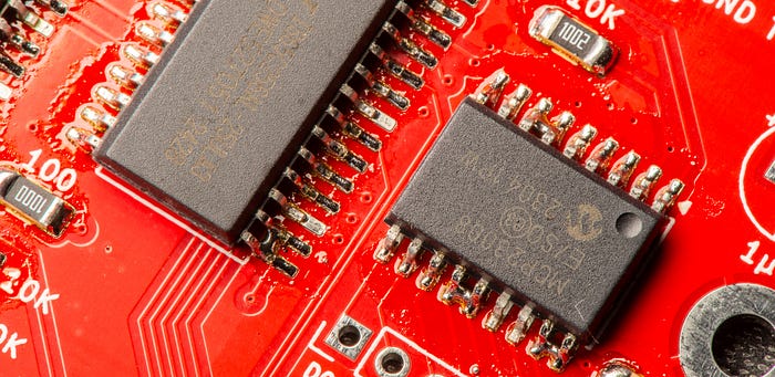
I like to help things along by using a wooden toothpick to scrape away the paste between the pins. On the SSOP parts (the RAM and port extenders) this worked a treat. On the tiny ATmega328PB, not so much. I wound up with a few solder bridges.
I poked at the bridges with a soldering iron fitted with a blade-like tip. I also removed excess solder using braid and finally did some reflowing with a hot air gun (with surrounding components protected with Kapton tape to prevent them blowing away). This left me with one, final, short. Alas, it was across +5V and ground. Not good.
As much as I stared at the board with all the magnification I could muster, I couldn't for the life of me see any bridge between those pins. Maybe the short was elsewhere?
My suspicion immediately fell on the many 1206 bypass capacitors. They all connect to both +5V and ground. And too much solder paste could perhaps have formed a bridge under the component. So I removed all the capacitors, one by one, checking to see if the short was still there. It was. So much for that idea.
Finally I removed the ATmega328PB and there it was — a tiny solder ball between two pads, invisible when the chip was in place.
By this time, the chip and the board were a mess. I'd even managed to lift a pad in my frustrated and arguably over-aggressive use of the knife-tipped iron. Time to move on and try again. I suspect this is the real reason PCB fab houses have a minimum order of five copies.
If in doubt, add flux
There's an established principle in the electronics world that goes something like: 'If you're having soldering problems, you need more flux'. Or words to that effect.
The next time, I ran a flux pen over the pads for the ICs before applying paste. This was a mistake. Do not try this at home. The solder paste had trouble adhering to the pads and would just slide off. It also then just spread out, dissolving into a puddle, making a mockery of my attempts to scrape between the pads.
In the interests of science, I went ahead and added all the surface mount components and popped it in the oven. My hopes weren't high. The result?
Bridges.
Bridges as far as the eye could see. Those on the SSOP ICs cleaned up easily with the soldering iron knifing technique. With the microcontroller I alternated between using braid and (gentle) knifing and soon those bridges were gone too.
So it worked out in the end, but I'll never use that 'flux first' technique again. I'll go back to my original scraping technique but will put flux on to the legs off the ICs at the last minute. I'll let you know in the Lab Notes newsletter how that goes.
And I may consider ordering a stencil for any board with a TQFP component in future. Or, perhaps, get PCBWay to add the components during manufacture with its PCB assembly service.
The good news is that the board works as advertised. I need to clean it up (you may have noticed the flux in some of the images above). I'm saving my pennies for an ultrasonic cleaner.
The bad news is that the process of burning a ROM image to the flash is not fast. It takes about 19s to upload the 16KB ROM image to RAM. And then it's another 1m 40s to write the data to the flash. Yikes!
That said, two minutes for the whole process is competitive with the old method of juggling EEPROMs and the new way doesn't involve me getting out of my chair, which is a big win.
However, I do need to play with the software (there's at least one bug). And I do have ideas for other approaches. I'll get into all that in future articles.
There's a GitHub repo for this flash programmer project, which includes schematics and Gerbers for the PCB, C++ code for the ATMEGA328PB and Python code for the PC.
Many thanks to PCBWay for supporting Machina Speculatrix by supplying free PCBs.
The articles relevant to this project are:
- Using flash memory as a homebrew computer ROM.
- A development board for flash-based ROM (this article).
I will add others to this list as they are published.
Steve Mansfield-Devine is a freelance writer, tech journalist and photographer. You can find photography portfolio at Zolachrome, buy his books and e-books, or follow him on Bluesky or Mastodon.
Sign up for the Machina Speculatrix Lab Notes newsletter.
You can also buy Steve a coffee.
My Friend retro games NES SEGA