PROGRAMMING
So here's the idea. The process of burning new code into an EEPROM can be tedious. When you're developing the ROM code for a homebrew microcomputer, you find yourself doing this over and over.
It takes time and effort. It eventually wears out the EEPROM and as it involves constantly removing and reinserting the chip, there's the ever-present danger of bending the legs (even with a ZIF socket) or inserting the chip backwards (ask me how I know).
It would be so much easier to have the software toolchain simply upload the new firmware to the computer directly. After all, that's typically the workflow with microcontrollers such as the Arduino.
Enter flash
How do microcontrollers do this? The answer is that the program code gets stored in flash memory. Like a ROM or EEPROM, this is non-volatile, so the contents remain intact even when the device is powered down.
So the answer is simple. You just replace the EEPROM with a flash chip and you're good to go. I've encountered homebrew machines that have done this and mightily envied them. There's just one problem.
See above where I used the word 'simple'? Well, maybe it is if you know how to program flash chips. I didn't and so I decided to find out, and share my experience with you.
Choose your chip
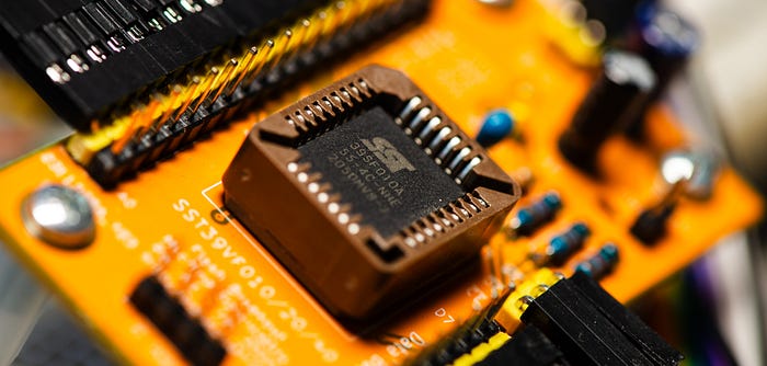
The first step is selecting a flash memory device. I opted for the Microchip SST39SF010A because I saw it being used a lot, it's well documented and crops up a lot in forum discussions, meaning that there's a readymade support network out there. Don't ask me to justify it beyond that.
The device is available in a compact 32-pin PLCC format. Even when socketed, this doesn't take up too much room on a circuit board. On Mouser.fr you can pick them up for about 1.70€ a pop, which is adorably cheap.
(Just an aside: Although my copy of the data sheet doesn't mention it, the chip is also available in a 32-pin PDIP package, which fans of through-hole parts might appreciate. I discovered — after having started writing this article — that I have several of these chips, still in their packing tube. This is the inevitable result of a dull evening and idle browsing on Mouser with the search page open and the shopping cart not quite at the 50€ minimum for free delivery. But I digress.)
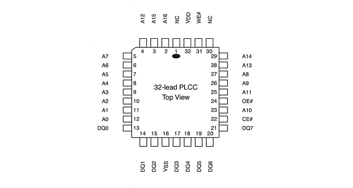
This is a 5V chip, but 3.3V variants are available, if that's the way you prefer to go. The chip has a read access speed of 55ns, which is actually much better than the 150ns of the Atmel AT28C256 EEPROM I'm currently using in the Zolatron homebrew microcomputer. And it has a capacity of 1Mbit, or 128KB in real money. This is far more than I need, but I have vague idea of maybe storing several ROM images in the one chip (I could put eight of them in there) and selecting between them with a switch. But that's for future me to worry about.
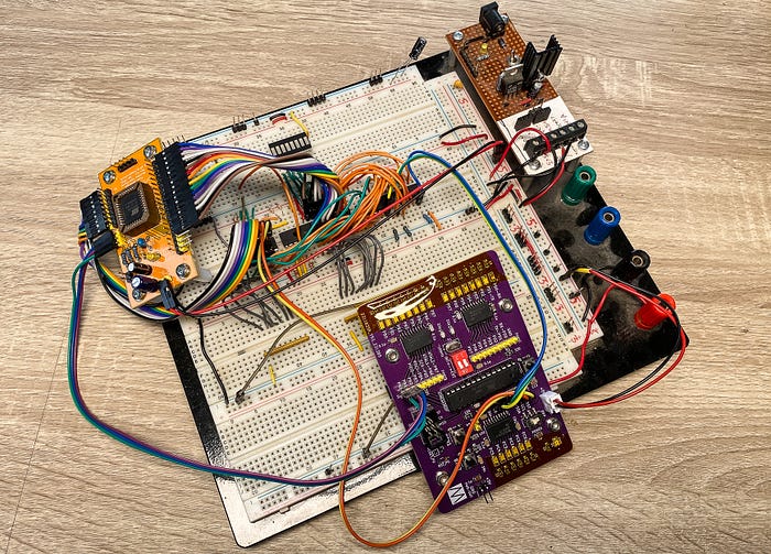
Whenever I start messing with a new device like this, one of my first steps is to create some kind of breakout board, or prototyping board. For this project I wound up using two I'd already made — one for an ATMEGA328P microcontroller and the other for the flash chip. The microcontroller board could be replaced by an Arduino or the MCU of your choice.
Dev board architecture
In principle, writing to a memory chip is simple. You wire the chip's pins to the GPIO pins of, say, a Raspberry Pi or microcontroller. You put the value of a byte on the data bus pins, the value of an address on the address bus pins, set the flash device's chip enable pin appropriately and also set the write enable. Do the same for the next byte and the next. Rinse and repeat.
Well, that's how something like RAM works, but flash isn't quite so easy. Of course it's not.
For one thing, before writing to flash memory you have to erase it. And not byte by byte but sector by sector (or page by page, according to which term the chip manufacturer prefers).
Let's see what the datasheet has to say under the heading 'Byte-Program Operation':
Before programming, the sector where the byte exists must be fully erased. The Program operation is accomplished in three steps. The first step is the three-byte load sequence for Software Data Protection. The second step is to load byte address and byte data. During the Byte-Program operation, the addresses are latched on the falling edge of either CE# or WE#, whichever occurs last. The data is latched on the rising edge of either CE# or WE#, whichever occurs first. The third step is the internal Program operation which is initiated after the rising edge of the fourth WE# or CE#, whichever occurs first.
See what I mean by not so simple? But don't worry, we'll break this down into easy stages.
The key takeaway here is that writing to flash is not at all like writing to RAM. You can't just change a single byte. If that's what you want to achieve, you'd need to read the whole sector where the byte is meant to go, change that one value, then write the whole sector back again. That might not be too onerous with flash chips that have small sectors (some are as small as 64 bytes), but the SST39SF010 has a 4KB sector size.
However, if your plan is like mine — to write an entire ROM image to flash — this isn't an issue.
Intermediate step
I decided on a particular, and perhaps peculiar, approach to writing these flash chips.
Somehow, the data needs to be pushed from an origin (my dev computer) to the chip. My MacBook doesn't have GPIO pins. I could have used a Raspberry Pi as the dev platform but, for various reasons, that doesn't give me the benefit of being able to code while lying on the living room sofa.
So some sort of intermediary would be required — one that could accept data from the laptop and then handle the interface with the flash chip. This, clearly, is a job for a microcontroller, and I just happen to have a few dozen of those lying around. Maybe more.
The interface between this and the laptop would be simple — a serial connection. Then the MCU would be wired (almost) directly to the flash chip.
But because of all that sector erasing business, you can't just push the data in one chunk.
This suggested to me two main approaches:
- Some form of flow control, in which a sector's worth of data would be pushed at a time from the PC, followed by a suitable pause for writing; or
- An intermediate buffer.
So what's the plan?
This is what I came up with. I would build a device with an ATMEGA328PB microcontroller that connects to the computer via serial. (My initial experiments were with the ATMEGA328P, but that's changing.) The MCU receives the data in one big gulp and stores it to local SRAM. Then, on a command from the computer, it writes the data, sector by sector, to the flash chip.
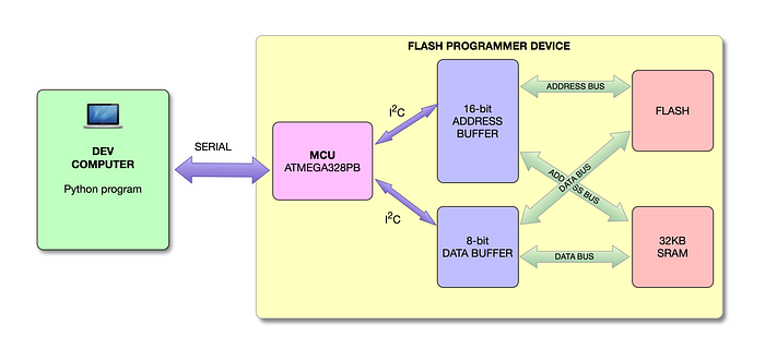
On the computer end, I have a Python program that allows me to select a file, push it to the device and then command it to carry out the write operation.
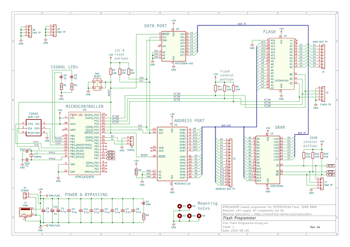
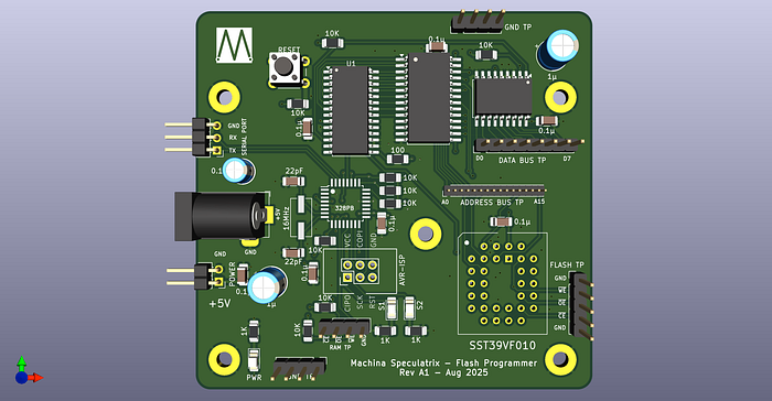
In future articles, I'll get into the full details of the device and the software involved. As a teaser, here's the current state of the schematic for the device (it may change).
You may notice the presence of an MCP23008 and MCP23017 port expander chips. I'm using these to provide the 24 pins I need for a 8-bit data bus and 16-bit address bus.
And here's a Kicad render (also subject to change).
For now, I'm using a breadboard plus the prototyping/breakout boards I made for the flash chip and the ATMEGA328P. This works, but is an unholy mess. That's why I'm playing with designing the device above.
Burning data
As is so often the case with ICs, the behaviour of the SST39SF010 flash chips is governed by your manipulation of three key signals: chip enable (/CE), output enable (/OE) and write enable (/WE). All are active low and you'll almost certainly want to put pullup resistors on these lines. I find 10KΩ works a treat. By the way, the datasheet indicates they are active low with the hash symbol but I prefer the leading slash.
The chip does nothing of any interest unless /CE is low. When it's high, the chip is in a low-power standby state and the data bus goes high impedance.
Whether you read or write data is dependent on the other two signals.
You also need to give the chip a number of commands. Here's the datasheet again:
Commands are used to initiate the memory operation functions of the device. Commands are written to the device using standard microprocessor write sequences. A command is written by asserting WE# low while keeping CE# low. The address bus is latched on the falling edge of WE# or CE#, whichever occurs last. The data bus is latched on the rising edge of WE# or CE#, whichever occurs first.
Put more simply, when you put the chip into write mode (with first /CE and then /WE being taken low), the chip assumes that the first thing it's going to see on the data and address buses is a command. In fact, it assumes it's receiving a command sequence that may, or may not, include data to write to memory.
In sequence
To make things clearer, let's look at some sequences.
To send the chip a command, perform the following write operation:
- Take
/CElow. - Put a special command address on the address bus.
- Put a special value on the data bus.
- Pulse
/WElow and then high again —a low duration of 20µs works well. - Take
/CEhigh again.
As we'll see, the two special addresses are 0x2AAA and 0x5555. The flash chip knows to look out for these.
But just one command isn't going to do it. Like I said, it expects a sequence.
Sector erase
Here's how you erase a sector:
- Perform the above write operation with address
0x5555and data0xAA. - Write with address
0x2AAAand data0x55. - Write with address
0x5555and data0x80. - Write with address
0x5555and data0xAA. - Write with address
0x2AAAand data0x55. - Perform a write operation with the start address of the sector you want to erase on the address bus and
0x30on the data bus. - Pause to let things take effect. I've found 25µs works.
In case you're wondering about the values 0x55, 0x80 and 0xAA, their binary representations give a hint as to why they were chosen. Here are the bytes in hex and binary:
0x55   01010101
0xAA   10101010
0x80   10000000
Presumably, those simple patterns (especially with 0xAA being the inverse of 0x55) made for easier hardware logic within the chip.
Writing bytes
With a sector erased, you can now write as many bytes as you like to it (within its 4KB capacity, of course).
To write a byte:
- Perform a write operation with address
0x5555and data0xAA. - Write with address
0x2AAAand data0x55. - Write with address
0x5555and data0xA0. - Write with the address of where you want to write the byte and the data bus set to the byte value.
There's a couple of other operations you can achieve via command sequences, such as erasing the whole chip or writing an ID code to it. But I'll leave those as exercises for the reader (because you are going to read the datasheet, right?).
Reading a byte
Reading is simple — basically the same as for any ROM or RAM chip. This is why a flash chip makes a good candidate for replacing an EEPROM.
- Take
/CElow to enable the chip. - Put the address of the byte you want to read on the address bus.
- Take
/OElow to enable output. - Read the byte.
- Take
/OEhigh again. - Optional: Repeat steps 2–5 for any further bytes you want to read.
- Take
/CEhigh again.
Not too difficult
And that's largely it. It's not all that difficult, but those command sequences and the need to erase sectors can be a little daunting when you first encounter them.
And you have to pay attention to timings (as always, the datasheet is your friend) to ensure that actions have time to complete.
In the next article on this topic, I'll go through the circuit I built to write a ROM image for the Zolatron homebrew computer to a flash chip and give a deeper insight into the code.
Future plans
I have in mind to respin the main CPU board for the Zolatron. I'd be adding the microcontroller, replacing the EEPROM with the flash chip and using the computer's existing RAM as the write buffer. At least, that's the idea. Let me know if you think I'm crazy.
There's a GitHub repo for this project. NB: It's a work in progress.
You can find all the stories related to my homebrew computer project on the Zolatron feature page.
There is also a GitHub Zolatron repo with the code, datasheets and other documents.
Steve Mansfield-Devine is a freelance writer, tech journalist and photographer. You can find photography portfolio at Zolachrome, buy his books and e-books, or follow him on Bluesky or Mastodon.
You can also buy Steve a coffee. He'd like that.
My Friend retro games NES SEGA